0 Preface
Since 1987, the literature [1] firstly used aromatic diamine derivatives as hole transport materials, and 8-hydroxyquinoline aluminum (Alq3) as the light-emitting layer material to prepare organic light with high efficiency, high brightness and low driving voltage. Since the Organic Light-Em Iting Diode (OLED), it has received great attention due to its low power consumption, high brightness, wide viewing angle, fast response, etc., organic electroluminescence (Emissive Layer, EL) Research has become one of the hot spots in the field of current luminescent display. A lot of research work has been carried out from luminescent materials, preparation processes, luminescence mechanism, device structure and other aspects. The photoelectric performance of the device has been significantly improved, but the luminous efficiency and brightness of the device are still the bottlenecks hindering the commercialization of OLEDs. one. In order to improve the photoelectric performance of the light-emitting device, polyvinyl carbazole (PVK) was used as the hole transport material, and Alq3 was used as the electroluminescence/electron transport material to prepare the structure of Indium Tin Oxide (ITO)/PVK. /Alq3/Mg: Ag/Al OLED device, the effect of hole transport layer thickness on the photoelectric performance of the device was studied, the thickness matching of the device functional layer was optimized, and the structure-optimized OLED device was obtained.
1 experiment
1.1 Materials
ITO conductive glass (15Ω) was selected as the anode material of the OLED device. High-purity magnesium metal (99.9%), silver (99.9%) and aluminum (99.999%) were used as cathode materials for the device. PVK was used as the hole transport layer material of the device. Alq3 is used as the light-emitting layer and electron transport layer material of the device. These organic materials are all purchased from Aldirch, USA, and the molecular structure can be found in the literature [1-3].
1.2 ITO substrate surface treatment
Before preparing the OLED device, the ITO substrate was ultrasonically cleaned with detergent, acetone solution, NaOH solution, ethanol solution, and deionized water for 20 min, then dried by high-purity nitrogen, and placed in an OLED-V type organic multifunctional film. In the pretreatment chamber of the apparatus, oxygen plasma treatment was performed at a voltage of 250 V for about 30 minutes.
1.3 OLED device preparation
Different concentrations (2, 3, 6, 9 mg/m1) of PVK/chloroform solution were spin-coated at 4 000 r/min (time 60 s) to clean the ITO substrate to obtain different thicknesses, l5, 30, 60 nm) PVK film. All PVK films obtained by spin coating were baked under vacuum for about 30 minutes to remove residual solvent from the film.
Finally, when the degree of vacuum is 10-4 Pa, the organic layer Alq3, the alloy cathode layer Mg: Ag (10:1) and the metal layer Al are sequentially deposited by thermal evaporation. The alloy Mg:Ag was prepared by a two-source co-steaming technique, and the evaporation rate and film thickness were monitored by a quartz crystal oscillator. The evaporation rates of the organic layer and the metal layer are 0.2-0.4 nm/s and 2-4 nm/s, respectively. The thickness of each functional layer and the fabricated OLED device structure are ITO/PVK (O-60nm)/Alq3 (60 nm). ) /M g: Ag (100 nm ) / Al (150 nm ).
1.4 OLED device performance test
The voltage, current, brightness and spectrum of all unpackaged OLED devices were performed using KEITHLEY-4200 semiconductor tester, ST-86LA screen luminance meter and OPT-2000 spectrophotometer at atmospheric and room temperature (25 ° C). test.
2 Results and discussion
2.1 Influence of hole transport layer thickness on device electro-voltage characteristics
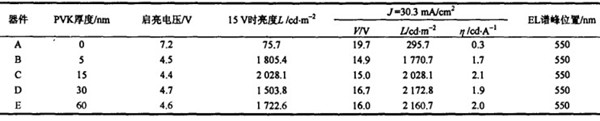
Figure 1 shows the current-voltage (JV) characteristics of a hole-transport layer device with different thicknesses. The letter A represents a single-layer device, and the letters B, C, D, and E represent PVK thicknesses of 4, 15, 3, 60 nm, respectively. OLED device. It can be seen from Fig. 1 that the current density of all devices shows a steady increase with the increase of the driving voltage, and the current density does not monotonously decrease as the thickness of the hole transport layer PVK increases. When the forward bias voltage is less than 8 V, the applied voltage increases, and the change of current density is not obvious; when the applied voltage increases to a certain extent, the current increases rapidly. When V = 15 V, the current densities of devices A, B, C, D, and E are 7.2, 31.0, 30.3, 22.7, and 24.6 mA/cm2, respectively. At the same voltage å’, the current density through the device is determined by the relationship B > C > E > D > A . Since PVK is an excellent hole transporting material, its introduction effectively improves the recombination of carriers in OLED devices, making the current density of double-layer devices significantly larger than that of single-layer devices. At the same time, for the double-layer O LED, although the introduction of the hole transport layer PV K helps to improve the carrier recombination in the device, the increase in the thickness of the PVK increases the series resistance of the device. Therefore, the current density of the device is maximized only when the thickness of the PVK is appropriate.
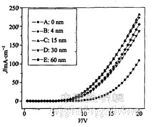
Figure 1 Curves of different thickness hole transport layer devices
2.2 Effect of hole transport layer thickness on device LV characteristics
Figure 2 shows the LV characteristics of all OLED devices. It is clear that the thickness of the hole transport layer significantly affects the turn-on voltage and luminance of the device. It can be seen from the figure that the turn-on voltages of devices A, B, C, D, and E are 7.2, 4.5, 4.4, 4.7, and 4.6 V, respectively, where device C has the lowest turn-on voltage and device A has the highest turn-on voltage. . When the forward bias voltage is less than 8 V, the illuminance brightness of the device is not significantly changed with the applied voltage. When the applied voltage V is greater than 8 V, the illuminance brightness of the devices C and D increases rapidly with the purpose, but the device The change in the brightness of A is not obvious enough. When the applied voltage V is the same, there is a big difference in the luminance L of the device. For example, when V = 15V, the luminances of the devices A, B, C, D, and E are 75.7, l805.4, 2408.1, and l503, respectively. 8. l722.6 cd/m2, the OLED brightness of the same voltage is C > B > E > D > A. It is easy to find that device C has the highest luminance. When V=20 V, the value of L is close to 5557.5 cd/m2, which is much higher than other OLED devices.
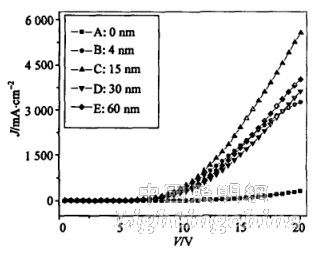
Figure 2 LV curves of different thickness hole transport layer devices
2.3 Effect of hole transport layer thickness on η-V characteristics of devices
The η-V characteristic curves of the hole-transport layer devices of different thicknesses are shown in Fig. 3. It can be seen that the current efficiency of all the double-layer devices is significantly better than that of the single-layer devices. When the applied voltage V=13.5 V, the values ​​of devices A, B, C, D, and E are O.33, 1.77, 2.29, 1.96, and 2.08 cd/A, respectively, which indicates that the current efficiency η of the two-layer device is a single layer. 5 to 6 times the device.
In addition, it can be seen from the figure that the total change trend of η first increases rapidly with increasing V. When V increases to a certain extent, η reaches a maximum value, and then η gradually decreases with increasing V. The maximum current efficiencies ηmax of devices A, B, C, D, and E are 0.39, 1.77, 2.42, 1.99, 2.1 lc, and d/A, respectively, where ηmax of device A is the smallest and C is the largest. The curve of the effect of the hole transport layer PVK thickness on the device ηmax is shown in FIG.
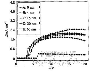
Figure 3 η-V curve of hole transport layer devices with different thicknesses
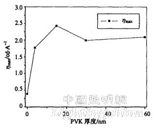
Figure 4 Curve of the effect of the thickness of the hole transport layer PVK on the device ηmax
Table 1 compares the main performance indicators of each device. It can be seen that on the one hand, the performance of the two-layer device is significantly better than that of the single-layer device. On the other hand, the thickness of the hole transport layer has a significant influence on the photoelectric performance of the OLED device. Overall, device C performs best with the lowest turn-on voltage, highest luminance, and luminous efficiency.
Table 1 Comparison of performance parameters of each device
For a bipolar injection OLED device, the intensity of the luminescence is proportional to the number of electron-hole pairs, ie:
 (1)
(1)
Where N and P are electron and hole concentrations, respectively; ηq is the efficiency of electroluminescence; r is the proportionality factor. It can be seen that the larger the phase difference between N and P, the smaller the luminance L of the light emission; the closer the N and P are, the larger the luminance L is: and when N = P, the luminance L reaches the maximum. As can be seen from the device level diagram shown in Figure 5, for the device ITO/AIq3/Mg: A g/Al, the electron injection barrier is 0.5 eV and the hole injection barrier is 0.9 eV. Therefore, the injection of electrons and holes is extremely unbalanced during the operation of the device, and the values ​​of N and P differ greatly. It is known from equation (1) that the photoelectric performance of such devices is poor. However, for the device ITO/PVK/Alq3/Mg:Ag/Al, when the PVK hole transport layer is introduced, on the one hand, the hole injection barrier is reduced (0.7 eV) to improve the hole injection capability, and on the other hand, The Alq3~PVK interface forms a high barrier barrier, which is beneficial to confine the electrons injected from the cathode to the luminescent layer (Alq3) and effectively recombine with holes, which improves the recombination efficiency of carriers in the device and improves the efficiency. The performance of OLEDs, so the photoelectric performance of these devices is significantly better than the device ITO / Alq3 / Mg: Ag / Al.
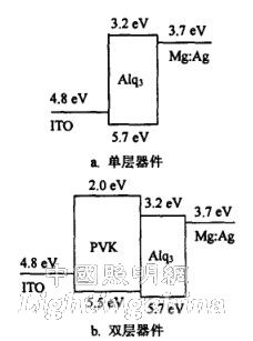
Figure 5 shows the energy level structure of the device
3 Conclusion
In this paper, a series of ITO/PVK/Alq3/Mg:Ag/Al organic light-emitting devices were fabricated. By testing and analyzing the photoelectric properties of the device, the effect of hole transport layer thickness on the performance of OLED devices was studied, and the device functional layer was optimized. The thickness is matched. The experimental results show that the photoelectric performance of the two-layer device is significantly better than that of the single-layer device, and the thickness of the hole transport layer also has a significant effect on its photoelectric performance. When the hole transport layer has a thickness of 15 nm, the double-layer device has better device performance, and has the lowest starting voltage, and the highest luminance and luminous efficiency.
Edit: Cedar
The photoelectric switch is the abbreviation of the photoelectric proximity switch. It utilizes the shielding or reflection of the light beam by the detected object, and the circuit is connected by the synchronization loop to detect the presence of the object. The object is not limited to metal, all objects that can reflect light (or block light) can be detected.
Photoelectric Proximity Sensor,Photoelectric Switch Sensor,Photoelectric Proximity Switch,Infrared Photoelectric Switch Sensor
Changchun Guangxing Sensing Technology Co.LTD , https://www.gx-encoder.com