Temperature is a physical quantity that characterizes the degree of heat and cold of an object. It is one of the most common and basic parameters in industrial production. Temperature monitoring is often required during production. The traditional temperature acquisition system usually uses a single-chip microcomputer or a digital signal processor DSP as a microcontroller to control the operation of the analog-to-digital converter ADC and other peripheral devices; however, the high-speed multi-channel temperature acquisition system based on single-chip microcomputer or DSP has certain insufficient. Since the clock frequency of the single-chip microcomputer is low, and the single-chip microcomputer is based on the sequential language, various functions must be realized by the operation of the software. Therefore, as the program quantity increases, if the program is not robust, a program runs. Fly and reset. The operation speed of DSP is fast, and the processing of complex multiplication and addition operations has certain advantages, but it is difficult to complete the complex hardware logic control of peripheral devices. Therefore, the microcontroller or DSP is difficult to meet the requirements of real-time and synchronization when performing multi-channel temperature acquisition in complex industrial sites. In view of this, this paper introduces a multi-channel real-time temperature acquisition system based on SOPC technology. The system has a short development cycle, flexible resource allocation and good stability, and meets the application in the industrial production field with high requirements for real-time and synchronization of temperature acquisition.
1 The overall structure of the system
The hardware of the temperature acquisition system is mainly composed of temperature acquisition module, data storage module, FPGA logic control module and communication module. The overall structure is shown in Figure 1.
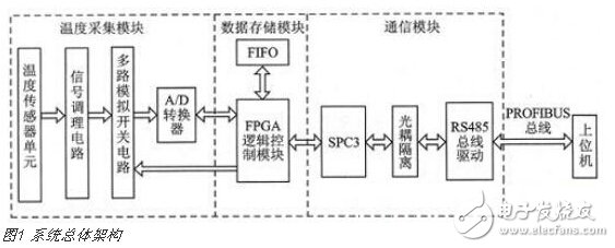
After the system is powered on, the configuration data is automatically loaded into the SDRAM (HY57V641620) of the FPGA (Cyclone II series EP2C8Q208C) by the static memory EPCS16, and the digital logic circuit solidified therein is mapped into the FPGA device. The temperature sensor unit AD590 first collects the temperature signal and then processes it through the signal conditioning circuit so that the output amplitude of the signal satisfies the range requirement of the A/D sampling. At this time, the FPGA controls the analog selection switch ADG706 to perform channel selection, and simultaneously controls the multi-chip 16-bit A/D converter ADS8402 for A/D conversion, and stores the collected real-time data in a time-sharing manner to two types of FIFOs with a capacity of 16K & TImes. 9-bit memory IDT72V06. Then, the data in the IDT72V06 in the read state is read out, and the SPC3 communication module is controlled by the FPGA, and transmitted to the upper computer through the PROFIBUS bus.
2 Temperature acquisition system design
2.1 Temperature Acquisition Module
The temperature acquisition module consists of four parts: temperature sensor unit, multi-channel signal conditioning circuit, multi-channel analog switch circuit and multi-channel A/D converter.
The temperature sensor unit uses a thermocouple. It has the following advantages: wide temperature measurement range, stable performance; high measurement accuracy, direct contact between thermocouple and the object to be tested, independent of intermediate medium; fast thermal response time, thermocouple response to temperature changes; large measurement range, -40~+1600°C can measure temperature continuously; the performance is firm, the mechanical strength is good; the service life is long, and it is convenient to install. It is especially suitable for real-time detection of temperature in complex industrial production process.
The multi-channel analog switch circuit uses 16 analog select switches ADG706. The input of the 4-bit address bits .A0, A1, A2, and A3 is directly controlled by the I/O ports CH0, CH1, CH2, and CH3 of the FPGA, and the channels to be outputted among the 16 input signals are determined, and each channel selection command will be simultaneously Start the corresponding temperature acquisition channel of multiple ADG706s. Then start the corresponding temperature acquisition channel for A/D conversion. This design uses the high-speed successive approximation register (SAR) analog-to-digital converter ADS8402. The start conversion pin of the multi-chip ADS8402A/D converter shares an I/O port A/D Start of the FPGA. The data output control of the high and low byte control pins BYTE and ADS8402 of the ADS8402A/D conversion result is controlled by the separate I/O of the FPGA. Each FPGA sends a 100ns negative pulse to the A/DStart port to start multiple ADS8402 data acquisition on the corresponding channel. After the conversion is completed, the A/D conversion result can be read by controlling the BYTE port and temporarily stored in the corresponding data unit.
2.2 Data Storage Module
The multi-channel acquisition signal has a large number of channels and a large amount of processed data, and an external data storage module is needed to buffer the FPGA processing result. At the same time, due to the multi-tasking of the host computer, it is impossible to read data in a pair of parallel ports. In order to ensure that the FPGA control core communicates with the host computer to read large amounts of data at a time, the system uses two asynchronous FIFO chips IDT72V06. Its storage capacity is 16K & TImes; 9 bits, access time is 15 ns, one of which is used to store the collected data, and the other is used to read the collected data stored in the FIFO for parallel port communication with the host computer. During the system operation, two FIFO bits are extended for double-buffer ping-pong control, and the read and write operations are performed in turn, which can greatly improve the communication speed and data throughput of the parallel port.
2.3 Communication module
PROFIBUS-DP is an optimized high-speed, low-cost communication connection designed for communication between distributed control systems and device-level distributed I/O. It is used for high-speed data transmission in distributed control systems. High-speed data communication between the system and distributed peripheral I/O devices and intelligent field instruments. SPC3 integrates all PROFIBUS-DP protocols, and SP C3 will complete all DP-SAP settings in DP mode.
SPC3 integrates 1.5 KB of dual-port RAM, including parameter registers, mode registers, status registers, and interrupt controllers. The SPC3's integrated watchdog timer has three operating states: baud rate detection, baud rate control, and slave control. The internal USART enables mutual conversion of parallel data streams and serial data streams. The micro-sequence controller controls the entire working process, and the idle timer directly controls the serial bus timing. The communication module is designed with the PROFIBUS-DP dedicated communication protocol chip SPC3, which can speed up the execution of communication and reduce the burden on the microprocessor.
2.4 FPGA logic control module
The FPGA-based acquisition control unit uses a top-down modular design approach to design each control module using the Verilog HDL language. The FPGA logic control module includes an A/D sampling control module, a FIFO read/write control module, and an SPC3 control module.
2.4.1 A/D sampling control module
The A/D sampling control module is responsible for controlling the gating of the multi-channel analog input of the external ADS8402 chip and achieving reasonable control of the A/D sampling process.
Since the ADS8402 takes a time-sharing conversion of the 16-channel analog, channel selection is required at the same time as the conversion is initiated. The ADS8402 sets four channel address lines A0, A1, A2, A3, and an address latch enable signal ALE. When ALE goes high, the channel number determined by A0, A1, A2, A3 encoding is latched, and the analog quantity of the channel is connected to the A/D converter for conversion. According to such characteristics, a hexadecimal counter with a reset terminal is designed, and the count output terminals Q3, Q2, Q1, and Q0 are respectively connected to the four address lines of the ADS8402. The counter power-on reset to ensure that the system starts sampling from channel 0. The conversion end signal EOC of the ADS8402 is used as the clock signal of the counter, and the sampling control of the next analog input is automatically started after one-way conversion is completed.
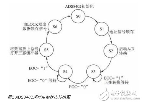
The control of the A/D sampling process is implemented by a finite state machine, which divides the sampling process of a channel into seven states, as shown in Figure 2. First, the S0 state initializes each control signal. The rising edge of the ALE signal is generated in the S1 state, and the channel address is latched. The start signal START should be generated on the same clock falling edge of the ALE signal. Since the VHDL language does not allow the two edges of the clock to be sensitive variables in the same process, the START signal is generated as a single state S2, and the conversion is initiated. After the conversion is initiated, the ADS8402 sets EOC low and sets the S3 state to wait for the A/D conversion to complete. After the conversion is completed, the EOC signal is converted from a low level to a high level, the state machine enters the S4 state, and the output enable OE is enabled. The state machine enters the S5 state, and the data latch signal LOCK is turned on to latch the data. To generate a signal that communicates with other processes, the state machine sets S6 as the last state and then jumps back to the SO initial state.
2.4.2 FIFO read and write control module
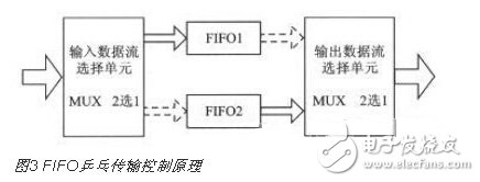
Two FIFOs are used for reading and writing operations to realize data caching between the FPGA and the PC. The schematic diagram of the principle of ping-pong transmission control is shown in Fig. 3. The solid arrow and the dashed arrow in the figure respectively represent different read and write data cycles. The input data stream is passed through the input data stream selection unit, and the data stream is isochronously allocated into the FIFO 1, FIFO 2. In the first buffer cycle, the incoming data stream is buffered to FIFO1. In the second buffer cycle, the input data stream is buffered to the FIFO 2 by the switching of the input data stream selection unit, and at the same time, the data of the first cycle of the FIFO1 buffer is sent to the selection of the output data stream selection unit. The data stream operation processing module is arithmetically processed. In the third buffer cycle, the input data stream is buffered to the FIFO 1 by the re-switching of the input data stream selection unit, and at the same time, the data of the second cycle of the FIFO 2 buffer is transferred by the output data stream selection unit. The data stream operation processing module is arithmetically processed. This cycle, repeated again and again.
2.4.3 SPC3 Control Module
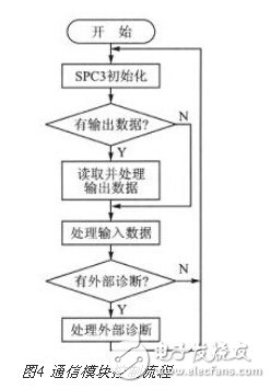
Since SPC3 integrates the complete DP protocol, the FPGA does not have to participate in the processing of the DP state machine when communicating. The main task is to transfer the data received by SPC3 according to the interrupt generated by SPC3, organize the data to be sent through SPC3, and organize external diagnosis as required. Before SPC3 works normally, it needs to be initialized to configure the required registers, including setting the interrupt permission of the protocol chip, writing the slave identification number and address, setting the SPC3 mode register, setting the diagnostic buffer, configuring the buffer, and the address buffer. , initialize the length, and according to the above initial value of the pointer of each buffer and the pointer of the auxiliary buffer. The control flow of the communication module is shown in Figure 4.
3 system FPGA implementation
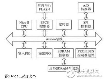
3.1 Nios II system architecture design
The Nios II system module includes: Nios II processor, Avalon bus, parallel I/O port PIO, serial peripheral interface SPI, timer TImer, on-chip memory EPCS, off-chip memory SDRAM, PROFIBUS-DP custom logic. Program control is performed by the Nios II processor, which is mainly responsible for temperature acquisition and data storage operations, and controls the communication process of PROFIBUS-DP. Its architecture is shown in Figure 5.
3.2 System Software Design
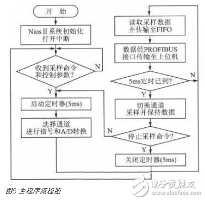
The software design of the Nios II processor is to store a written C/C++ language control program in the soft core. To control the system operation, it can read and write the memory unit of the chip while communicating with peripheral devices. In this system, the task of the Nios II program is: in a specified period, the FPGA receives the sampling task and control parameters sent by the host computer through the communication module, and then controls the analog selection switch ADG706 and the A/D converter ADS8402 to make them The analog signal of the selected channel is adjusted and A/D converted, and the sampled data is read and transmitted to the off-chip FIFO buffer by means of ping-pong transmission data, and then the sampled data is transmitted to the upper computer through the PROFIBUS-DP communication interface. The main program flow is shown in Figure 6.
Conclusion
The FPGA-based multi-channel real-time temperature acquisition system implements SOPC with the Nios II soft core processor, further simplifying the hardware design. Compared with the traditional MCU-based multi-channel temperature acquisition system, the system has the advantages of flexible resource configuration, stable and reliable operation, and strong real-time performance. In addition, the system has a standard PROFIBUS-DP interface, as a DP slave to achieve communication with a variety of DP masters, can be widely used in PROFIBUS distributed control systems in industrial production.
About Silicone Table Corner Protector
Silicone Table Corner Protector is one of our Silicone Kitchenware .There are many design on Silicone Corner Protectors.
Completely safe corner protector for your baby- Made of Food Grade Silicone.This product is 100% non-toxic and tasteless.Even if your baby bites the product,there will be no health risks.
Impact Absorbing- Soft,high-density premium cushions absorb impact provides maximum protection from sharp corners and edges.
Functionality- Sticks on Strong Baby Proofing Corner Guards and Corner Protectors,widely use on surfaces wood,glass,steel and ceramic.
Secure Adhesion:Strong 3M Adhesive and easy-to-peel,will not damage furniture.
Other type design silicone table corner protector can be clicked on Silicone Corner Guards , Silicone Edge Protector , Silicone Edge Guard ,Table Corner Protectors.
Product introduction:
1.Product name:Silicone Table Protector,Silicone Corner Protectors,Silicone Corner Guards,Silicone Edge Protector,Silicone Edge Guard,Table Corner Protectors
2.Place of origin:Guangdong China
3.Color:any pantone color
4.Effect:Any effect according to customer's requirement
5.MOQ:500pcs.
6.Package:1 pcs/opp,customized design is available.
7.Design:Customized/stock
8.Certification:FDA,LFGB,SGS,ROHS,etc.
9.Usage:Use for table corner,avoid being hit by the corner of the table
10.Silicone Table Corner Protector photos for reference.

Silicone Table Corner Protector
Silicone Table Corner Protector,Silicone Table Protector,Silicone Corner Protectors,Silicone Corner Guards,Silicone Edge Protector,Silicone Edge Guard,Table Corner Protectors
OK Silicone Gift Co., Ltd. , https://www.oemsiliconegift.com