With ON Semiconductor's NCP5604, it accurately drives a set of four LEDs in any display backlight or low-power flashlight with accurate matching current. After the output current is set by an external resistor connected to the IREF pin and ground, the enable pin directly controls the chip. This output provides a constant current to each LED, which rises to a set value within a few hundred microseconds, and the LED current is progressively started/stopped by means of a reference pin. This method of customizing the state of the lighting system is relatively simple and has been widely used. This application describes the progressive technology related circuitry.
Reference current
The output current is set by setting the reference current flowing into the external resistor. As shown in Figure 1, the internal subcircuit provides a bias voltage of 600 mV for the external resistor. The voltage on the IREF pin is regulated by an operational amplifier U1 connected to NMOS M3 and a 600 mV reference voltage generated from a precision built-in bandgap voltage reference. The current flowing through the external resistor R2 is mirrored by the PMOS M1 & M2, and the M1/M2 size is adjusted at the wafer level to obtain a ratio of 1:10. Thus, when M1 flows through 1 mA, the M2 drain can generate 10 mA.
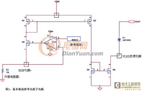
The current flows through the current mirror generated by the NMOS M4/M5. The net ratio of these two devices is 1:25, at which point 10mA can generate 250mA at the M5 drain. Since the external LED is connected to the drain, the current flowing into the LED is the drain current, and this value is only related to the product of the reference current set by the external resistor and the total ratio of M1/M5. ‖
Clearly, the sub-circuit is designed to support the reference current levels required in the application. Since the maximum load current per LED is 25 mA, the maximum reference current is 100 mA. If the external resistor drops below 5.2 kΩ, the reference current will drop and the LED current will not increase further, see the tolerances in the NCP5604 data sheet.
Power-on sequence
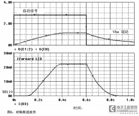
Assuming the chip is connected to the appropriate power supply (set Vbat to a minimum of 3V and a maximum of 5.5 V), the built-in system is activated when the enable pin is set high, see Figure 2. At this time, before the external storage capacitor is completed, no current flows through the LED, and the Vout voltage must be higher than the LED Vf before the forward current is generated. On the other hand, intentionally limiting the start-up input current of the battery, the rise time of the voltage on the storage capacitor is also limited, and it takes 200 ms to start the LED. Of course, for the naked eye, 200ms is extremely fast, and for the end user, the lighting is fleeting.
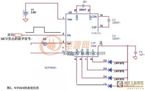
On the other hand, if the LED is turned off, or the forward current is turned off, the storage capacitor is slowly discharged: the converter will not restart from zero and the LED Vf can be reached without 200ms.
Progressive start/stop process
The basic concept is to gradually turn the LED on/off when the enable signal is set to high or low, without using the extra I/O pins on the MCU port. Since the chip does not have a programmable register integrated, it is not possible to provide this functionality in a purely digital way. An alternative is to use an analog structure that connects to the built-in reference current to control the LED current.
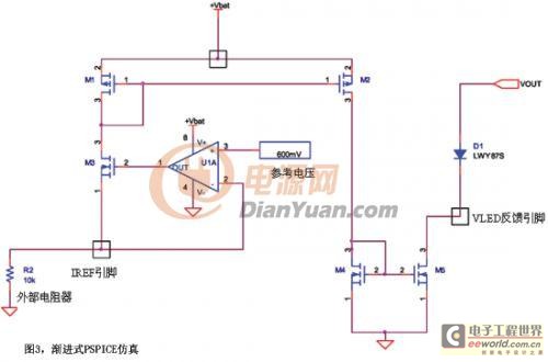
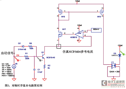
A simple application can be developed with an NPN transistor in a pseudo-mirror structure, forcing the reference current to flow into the IREF pin as shown in the PSPICE model of Figure 3. The current mirror represents the NCP5604 circuit, and the progressive function is implemented with transistor Q1 and the connected network. Resistor R2 forms the maximum reference current to achieve the maximum forward current flow of the LED. Basically, the enable signal is used to exponentially charge the capacitor C1 connected between the base/ground of transistor Q1. Once the voltage reaches transistor Vbe, the collector current flows, forcing the reference current slope to the desired time according to the R1/C1 network. Finally, the Q1 collector voltage is clamped by the constant voltage provided by the NCP5604 with a reference current of (Vref-Vcesat)/R2. In general, the collector/emitter voltage drop is small (range 50 mV) and can be ignored in applications where high accuracy is not required. ‖
However, taking this into account when calculating external resistors can properly compensate for this voltage drop. The waveform captured by the PSPICE model demonstrates this circuit characteristic (Figure 4).
Waveform captured by the PSPICE model
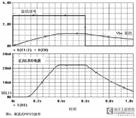
It can be seen that the curve at the time of closing is gentler than when it is turned on, because the reference voltages of the two time periods are very different. Although this is not a critical issue, some applications may require more symmetrical timing, which can be achieved by connecting additional resistors to the small signal diode. Figure 6 shows the waveforms based on the PSPICE basic circuit diagram of Figure 5, illustrating the performance that can be achieved by accessing D2 and R8.
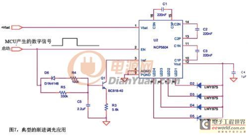
Typical applications are shown in Figure 7. Timing can be adjusted to handle different states. In any case, the delay capacitor (C5 in the circuit diagram of Figure 7) must be of a ceramic type to reduce leakage current, and low-cost electrolytic capacitors are not suitable for this application. As mentioned earlier, the incremental timing can be triggered without the extra input/output of the MCU, and the start signal can be used to implement both functions.
On the other hand, when the current reference resistor (R3 in the circuit diagram of Figure 7) is reduced to 5.6 kΩ, the Vcesat of transistor Q1 can be compensated.
‖
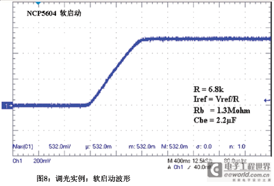
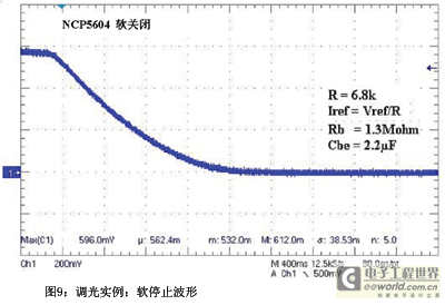
The waveforms in Figures 8 and 9 illustrate that when soft-start is generated using Rb = 1.3 MΩ/Cbe = 2.2 mF, the current output to the four LEDs is 25 mA. Of course, the ramp up delay can be increased or decreased by adjusting the Rb/Cbe network. However, Rb values ​​above 1.5 MΩ will cause the system to be sensitive to ambient noise. As mentioned earlier, Cbe capacitors cannot use low-cost electrolytic capacitors, and ceramic capacitors must be used to achieve the desired long timing.
A small signal NMOS device can be used in place of the external transistor Q1, such as the BSS138. Since the gate input does not sink current, a larger delay can be produced. Although it is also possible to run this application with smaller devices, the uncontrolled operating current caused by the large Rdson of the selected NMOS must be avoided. In fact, for devices with a Rdson rating of 5000 Ω, the above parameters change.