DDR3 is currently the mainstream product of DDR. The read and write separation of DDR3 is the most basic and most commonly used part of DDR. This paper mainly describes the method of DDR3 read and write separation. The first DDR, the chip is in TSOP package, the pins are exposed on both sides of the chip, it is quite convenient to test; however, DDRII and III are different, it uses BGA package, all solder joints are hidden in the chip At the bottom of the test, it is very inconvenient to test, and it is generally necessary to reserve test points in advance. Before the DDR read-write burst analysis, the read burst and the write burst must be separated first, and the two-way data is all placed on the DQS and DQ. So, in the DDR manual, what clues are left for us to write and separate? To achieve fast and easy separation of DDR, we must know the difference in characteristics between DDR read and write signals before reading and writing separation. First, take a look at the definitions in SPEC:
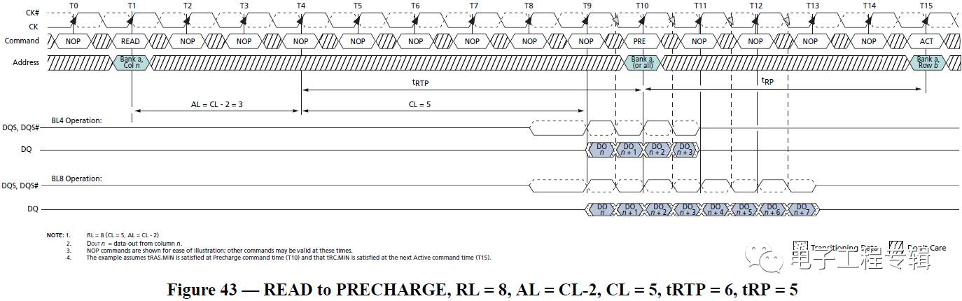
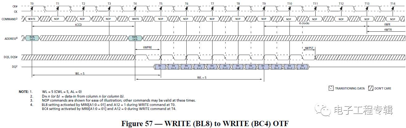
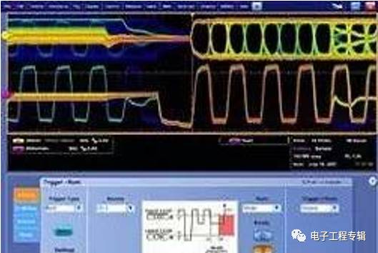
Method 1: Preamble difference Before each burst, DQS will switch from high impedance state to a negative pulse, and then normal reading and writing will begin. This negative pulse, we call it preamble (preamble is actually before reading and writing, DQS informs the DRAM chip or the controller's signal in advance). In general, the read data DQS has a preamble width greater than the write data. For DDR3, the situation is even simpler. Because in DDR3, the preamble of the read data is a negative pulse, and the preamble of the write data is a positive pulse.

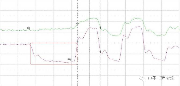
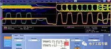
Method 2: The difference in amplitude is generally tested on the DRAM side. The data is written from the memory controller. After the motherboard PCB board, the memory slot and the memory board PCB board, when the DRAM particles arrive, the signal has been attenuated and read. The data just came out of the DRAM and has not undergone any attenuation, so the read data is larger than the write data. The method shown in the following figure three: write data is DQS and DQ centre-align (intermediate alignment), read data DQS and DQ are edge align (edge ​​alignment), memory controller receives DQS inside the controller when receiving read data in memory The phase of the DQ is shifted by 90 degrees to achieve intermediate alignment for sampling (the oscilloscope does not see this process); Method 4: Difference in slope: The slope of the read data is greater than the write data. Generally, the test is performed on the DRAM side, and the data is written from the memory controller. After the motherboard PCB board, the memory slot and the memory board PCB board, when the DRAM particles are reached, the signal has been attenuated, so the slope is also smaller; The data just came out of the DRAM and has not undergone any attenuation, so the slope of the read data is greater than the write data. You can also get a distinction from the picture below.
Accesories For Pc,Pc Casing,Pc Shell,RAM And SSD
Shenzhen Innovative Cloud Computer Co., Ltd , https://www.xcypc.com