4-channel class D audio amplifier principle and design
In a multi-channel design, driving each channel independently consumes more power, more components, and takes up more board space. As a result, temperature-related designs are complicated, and sound quality and reliability are lower at higher costs.
Therefore, in order to reduce the power consumption of high-performance multi-channel audio systems and simplify related temperature management as much as possible, design engineers have been hoping to use high-efficiency class D audio amplifiers that can provide over 90% efficiency over a wide range of output power levels. In contrast, the efficiency of traditional class AB amplifiers suitable for this market is only about 50%, and the efficiency will decline rapidly as the output power level decreases. Similarly, engineers continue to study the performance of integrated ICs to reduce the number of components and board area.
Whether in the automotive entertainment or home theater system market, consumers always require more channels and speakers, and each channel must be able to handle higher audio power levels. In addition to higher wattages, audiophiles continue to demand improved sound quality, reduced distortion and noise, and excellent isolation between channels.
4-channel driver
In response to this demand, International Rectifier (IR) has combined advanced DirectFET power MOSFETs with innovative integrated audio drivers to develop a 4-channel Class-D audio amplifier design with performance comparable to single-channel solutions. To achieve this goal, the circuit uses an integrated audio driver IRS2093M, which integrates four channels of high-voltage power MOSFET drivers on the same chip. In addition, this 200V device includes an on-chip error amplifier designed specifically for Class D audio amplifier applications in half-bridge topology, an analog PWM modulator, programmable preset dead time, and reliable protection (Figure 1). In addition to preventing direct current and current surges in the power MOSFET, the programmable preset dead time also enables a power design with scalable power and number of channels. These protection functions include overcurrent protection (OCP) and undervoltage lockout (UVLO) protection with automatic reset control.
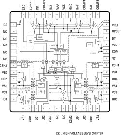
Figure 1: In addition to integrating the four channels of the high-voltage power MOSFETS driver on the same chip, this 200V device is also equipped with an on-chip error amplifier, analog PWM modulator, programmable preset dead time, and advanced protection functions.
In order to achieve first-class isolation between different channels, the audio driver deploys proven high-voltage junction isolation technology and a floating gate driver using the Gen 5 HVIC process. This achieves good internal signal isolation on the die, which allows the circuit to process more channels of signals at the same time, thereby keeping the basic noise of each channel at a very low level, while reducing the channel to channel as much as possible. Crosstalk.
Next, we constructed a 4-channel half-bridge Class D audio amplifier circuit as shown in Figure 2, which combines an integrated Class D audio controller and gate driver IRS2093M, with eight IRF6665 DirectFET power MOSFETs and several passive Device. Each channel of the multi-channel audio amplifier is designed to provide 120W of output power. For ease of use, this circuit contains all necessary internal management power.
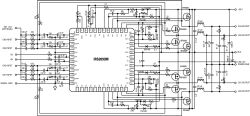
Figure 2: This 4-channel half-bridge Class D audio amplifier design uses an integrated Class D audio controller and IRS2093M gate driver, as well as eight IRF6665 DirectFET MOSFETs and some passive devices.
To achieve the best overall performance, the IRF6665 power MOSFET has been specifically optimized for the design of Class D amplifiers. In addition to providing low on-state resistance, power MOSFETs have been improved to obtain minimum gate charge, minimum body diode reverse recovery, and minimum internal gate resistance. In addition, compared to traditional wire-bonded packages, DirectFET packages can provide lower parasitic inductance and resistance. Simply put, the optimized IRF6665 MOSFET can provide high efficiency and low total harmonic distortion (THD) and electromagnetic interference (EMI).
Features and functions
In order to provide the highest performance and reliable design in a smaller space, this 4-channel Class D audio amplifier solution uses self-oscillating PWM modulation. Since this topology is equivalent to an analog second-order sigma-delta modulation and the class D switching stage is within the loop, the error in the audible frequency range is shifted above the inaudible frequency according to its operating characteristics, thereby reducing noise. At the same time, sigma-delta modulation allows designers to perform sufficient error correction to further reduce noise and distortion.
As shown in Figure 2, the self-oscillating topology incorporates a front-end integrator, PWM comparator, level switcher, gate driver, and output low-pass filter (LPF). Although this design can switch at a higher frequency, it still uses 400kHz as the optimal switching frequency for some reasons. First, at lower frequencies, the efficiency of the MOSFET has improved, but the inductor ripple current has risen and the leakage of the output PWM switching carrier has also increased. Second, at higher frequencies, switching losses will reduce efficiency, but there is a chance to achieve a wider bandwidth. When the inductor ripple current decreases, the iron loss will climb.
In a class D audio amplifier, the direction of the load current changes with the audio input signal, and the overcurrent condition may occur during a positive current cycle or a negative current cycle. Therefore, to protect both the high-side and low-side MOSFETs from overcurrent in both directions, programmable overcurrent protection (OCP) is used to provide bidirectional protection, and the RDS (on) of the output MOSFET is used as the current sensing resistor. In this design, when the measured current exceeds a preset threshold, the OCP logic will output a signal to the protection circuit, forcing the HO and LO pins to low level, thereby protecting the MOSFET from damage.
Due to the structural limitations of high-voltage ICs, the current-sensing deployment of high-side and low-side MOSFETs is different. For example, low-side current sensing is based on the VDS across the low-side MOSFET when the device is in the on-state. To prevent OCP from being triggered by instantaneous overshoot, a blanking interval is added after the LO is turned on to stop the 450ns overcurrent detection.
The threshold voltage for low-side overcurrent induction is set by the OCSET pin and ranges from 0.5V to 5.0V. If the VDS measured for the low-side MOSFET exceeds the voltage corresponding to the COM of the OCSET pin, the driver circuit will execute the OCP protection procedure. To set the over-current shutdown level, the voltage of the OCSET pin can be calculated using the following formula:

To minimize the effect of the input bias current on the OCSET pin, we selected resistor values ​​R4 and R5 so that the current flowing through the voltage divider reaches 0.5mA or more. At the same time, the VREF input to OCSET through a resistor divider improves the immunity to fluctuations in the power supply voltage Vcc.
Similarly, for positive load currents, the high-side overcurrent sensing also monitors the load conditions, at this time based on the VDS measured across the MOSFET during the high-side turn-on of the CSH and Vs pins. When the load current exceeds the preset turn-off level, OCP protection will stop the switching operation. To prevent OCP from being triggered by transient overshoot, a blanking interval can be added after HO is turned on to stop the 450ns overcurrent detection.
Unlike the low-side current sensing, the critical value of the CSH pin is internally fixed at 1.2V. However, a higher threshold can be set using external resistor dividers R2 and R3. Either way, an external blocking diode D1 is used to block the high voltage from flowing to the CSH pin when the high side is open. Based on a 0.6V forward voltage drop across D1, the minimum threshold for high-side overcurrent protection is 0.6V.
In short, the critical value VCSH of the CSH pin can be calculated by the following formula:
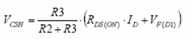
The ID in the formula is the leakage current, and VF (D1) is the forward voltage drop of D1. In addition, the reverse blocking diode D1 is forward biased via a 10kΩ resistor R1.
To prevent shoot-through or overshoot current from flowing through the two MOSFETs, we insert a blocking period called dead time between high-side turn-off and low-side turn-on, or between low-side turn-off and high-side turn-on. The integrated driver allows designers to choose a suitable dead interval from a series of preset values ​​based on the size of the selected MOSFET to optimize performance. In fact, only two external resistors are needed to set the dead time through the DT pin of IRS2093. This eliminates the need to use external gate timing adjustments and at the same time prevents external noise introduced by adjusting the switch timing, which is very important to ensure sound performance.
The user must consider the fall time of the MOSFET when determining the optimal dead time. This is because for practical applications, due to the relationship of the switch's fall time tf, the real effective dead time will be different from the data provided. This means that to determine the effective dead time, it is necessary to subtract the fall time of the MOSFET gate voltage from the dead time value in the data sheet.
Similarly, in terms of UVLO protection, the driver monitors the status of the voltages VAA and VCC before normal operation begins to ensure that both voltages are above their respective thresholds. If VAA or VCC is below the UVLO threshold, the protection logic of IRS2093 will turn off LO and HO. As a result, the power MOSFET will stop operating until VAA and VCC exceed their UVLO threshold.
In addition, in order to achieve the most ideal sound effect, the 4-channel audio circuit board design minimizes the line impedance and mutual coupling between the analog and switch sections, and ensures that the analog signal is separated from the switch stage and power ground.
Measured performance
We measured the efficiency, total harmonic distortion plus noise (THD + N) and EMI performance of each channel with a sinusoidal signal frequency of 1kHz, 1Vrms and 4Ω load impedance. In addition, we measured the 4-channel Class-D audio amplifier design shown in Figure 2 to show its best-in-class isolation and crosstalk performance. The power supply voltage of the relevant circuit board is ± 35V, and the natural frequency is 400kHz.
As shown in Figure 3, under a 4Ω load and a power output of less than 50W to 120W, the efficiency of each channel is about 90%. The main factors contributing to high channel efficiency include the DirectFET MOSFET IRF6665, which produces low on-state and switching losses. At the same time, because the integrated driver provides a safe dead time, the design does not have cross-conduction.
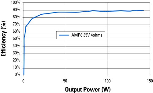
Figure 3: Under a 4Ω load, the power output is increased from less than 50W to 120W. The measured efficiency curve shows that the efficiency of each channel is about 90%.
This high efficiency allows this 4-channel design to handle one-eighth of the continuous rated power, which is the normal working environment required for general safety, without the use of any additional heat sinks or forced air cooling.
Similarly, tests conducted on distortion show that the THD + N performance of each channel is the same over a wide range of output power. As shown in Figure 4, when each channel is below 50W, THD + N will be less than 0.01%, and will increase as the output power rises. For example, when the output of each channel is about 100W, the degree of distortion will rise to 0.02%. This performance will be consistent throughout the audio range of 20Hz to 20kHz, even if the output power is increased from 10W to 50W per channel (under a 4Ω load). As shown in Figure 5, the fundamental noise of each channel is maintained below -80dBv throughout the audio range. Noise is measured at no signal input and 400kHz natural frequency.
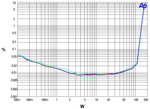
Figure 4: When each channel is less than 50W, the total harmonic distortion plus noise (THD + N) will be less than 0.01%, and will begin to increase as the output power increases.
Similar tests conducted for channel isolation showed that at 60W output power per channel, crosstalk between channels 1 and 3, and channels 1 and 4 is better than -70dB over the entire audio range.
At the same time, the design provides a good power supply rejection ratio (PSRR) of -68dB at a signal frequency of 1kHz. The high PSRR results from the natural frequency of the driver. This allows 4-channel Class D amplifiers to provide excellent performance even when using unregulated power supplies.
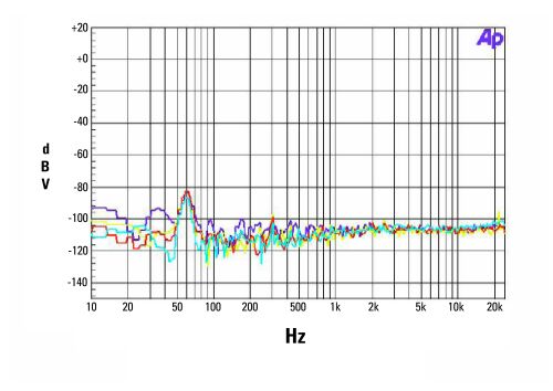
Figure 5: When no signal is input, the fundamental noise of each channel remains below -80dBv over the entire audio range.
Summary of this article
The 4-channel Class-D audio amplifier solution using the IRS2093M integrated driver can match the efficiency, THD + N, and EMI performance of a single-channel design. In addition, in the entire audible range, the fundamental noise remains below -80dBv. At the same time, there is excellent isolation between the channels to keep the intermodulation distortion (IMD) at a minimum level to provide ideal audio performance. With the high efficiency eliminating the need for heat sinks, the integrated audio driver has succeeded in realizing a 4-channel Class D audio amplifier solution with half the footprint.
RAM/RFM electric heating capacitors
RAM/RFM electric heating capacitors
Electric Heating Capacitor,Film Heating Capacitor,Electric Capacitor Bank,Induction Heating Capacitors
YANGZHOU POSITIONING TECH CO., LTD , https://www.yzpstcc.com