Prof. Zhou Ligong's new book, "Programming for AMetal Frameworks and Interfaces (Part 1)," provides a comprehensive introduction to the AMetal framework. By reading this book, developers can gain insight into highly multiplexed software design principles and interface programming techniques. The focus is on mastering your core domain, shifting your development mindset, and achieving mutual growth between the company and the individual.
Authorized by Professor Zhou Ligong, the Zhiyuan Electronic Public Number will serialize the content of this book, offering valuable insights to all readers.
The first chapter introduces the AM824-Core development kit. This section covers 1.1 LPC824 Microcontroller and 1.2 LPC84x Microcontroller.
This chapter guides:
With the rapid development of Internet of Things (IoT) technology, the capabilities of microcontroller units (MCUs) have significantly improved. The boundaries between modern MCUs and microprocessors are becoming increasingly blurred, and they are gradually being integrated into embedded processors. AMetal has completely abstracted the underlying complexity, allowing developers to focus only on the basic functions of the MCU.
1.1 LPC824 Microcontroller
>>> 1.1.1 Features
System:
- ARM Cortex-M0+ embedded processor with built-in nested interrupt vector controller (NVIC), system tick timer, and a maximum operating frequency of 30 MHz;
- Supports Serial Wire Debug (SWD) mode and JTAG Boundary Scan (BSDL) mode.
On-chip Flash and SRAM:
- Up to 32KB of on-chip Flash and 8KB of SRAM, with 64-byte page write and erase capabilities.
Digital Peripherals:
- Up to 32 general-purpose I/O pins with configurable pull-up/pull-down resistors, programmable open-drain mode, input inverter, and noise filter. GPIO direction control supports independent bit setting, clearing, and toggling;
- 4 pins with 20mA output drive capability and 2 open-drain pins with 20mA sink drive capability;
- GPIO interrupt generation capability with 8 GPIO inputs supporting Boolean pattern matching;
- Switch matrix for flexible configuration of each I/O pin function;
- CRC engine with DMA support for 18 channels and 9 trigger inputs.
Timers:
- State-configurable timer (SCTimer/PWM) for timing and PWM applications, with capture and match functionality;
- Quad Channel Multi Rate Timer (MRT) to generate repeatable interrupts at up to 4 programmable fixed rates;
- Self-wake timer (WKT) using an internal low-power oscillator or external clock;
- Window Watchdog Timer (WWDT).
Analog Peripherals:
- 12-bit ADC with up to 12 input channels, multiple internal/external triggers, sampling rate up to 1.2 Msamples/s, and support for two independent conversion sequences;
- Comparator with 4 input pins and internal or external reference voltage.
Serial Interfaces:
- 3 USART interfaces with switch matrix pin assignment and shared fractional baud rate generator;
- 2 SPI controllers with switch matrix pin assignment;
- 4 I2C bus interfaces, supporting high-speed mode plus, true open-drain mode data rate monitor, and up to 1 Mbps for high-speed I2C, and up to 400 kbps for standard I2C.
Clock Generation:
- 12MHz internal RC oscillator with ±1.5% accuracy for system clock;
- Crystal oscillator operating from 1MHz to 25MHz;
- Programmable watchdog oscillator with a frequency range of 9.4kHz to 2.3MHz;
- 10kHz low-power oscillator for WKT;
- PLL allows CPU to run at maximum frequency without requiring a high-frequency crystal, using system oscillator, external clock, or internal RC oscillator;
- Clock output with divider to reflect all internal clock sources.
Power Control:
- Integrated Power Management Unit (PMU) to minimize power consumption;
- Energy-saving modes: Sleep, Deep Sleep, Power Down, and Deep Power Down;
- Deep Sleep and Power Down modes can be awakened via USART, SPI, and I2C peripherals;
- Deep Power Down mode can self-wake via timer control;
- Power-on Reset (POR), Brownout Detection (BOD).
Single power supply (1.8V–3.6V), operating temperature range -40°C to +105°C.
>>> 1.1.2 Overview
The LPC824 series of microcontrollers (MCUs), as shown in Figure 1.1, features a rich set of on-chip peripherals, including a switch matrix, state-configurable timers, multi-rate timers, window watchdog timers, and DMA control. Analog peripherals include a 12-bit high-speed ADC and an analog comparator, along with three UARTs, two SPIs, and four I2Cs. An internal 12MHz RC oscillator is also integrated, serving as a clock source for the system.
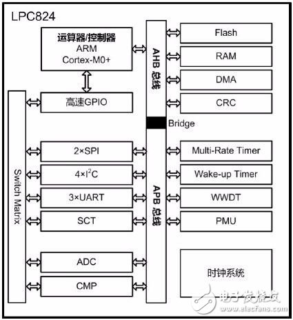
Figure 1.1 LPC824 Functional Block Diagram
The LPC824 Series MCUs are known for their ultra-low power consumption, with industry-leading performance of 90µA/MHz. They support four low-power modes, allowing users to choose the most suitable mode based on application needs. In the lowest power mode, the current consumption is less than 1µA.
Although these technical details may seem complex to beginners, don’t worry—just like how you use a computer without understanding its inner workings, you can still develop and program effectively with these MCUs.
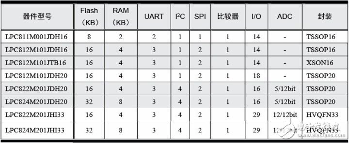
The LPC812/824 belongs to the LPC800 series. The LPC824 is an enhanced version of the LPC812, featuring more peripheral resources that better suit various application scenarios. Since the register configurations for the same peripherals are consistent, software design remains fully compatible, reducing platform construction complexity and allowing reasonable selection based on different needs. See Table 1.1 for details.
Table 1.1 LPC800 Series MCU Selection Table
The LPC824 series MCUs are available in two packages: TSSOP20 and HVQFN33, with pinouts as shown in Figure 1.2.
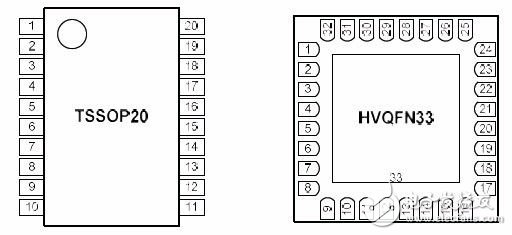
Figure 1.2 Schematic diagram of the package
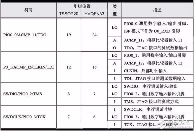
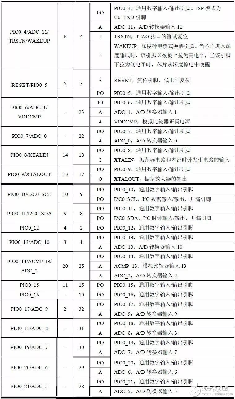
The pin descriptions and main functions of the LPC824 series MCU are shown in Table 1.2.
Table 1.2 Pin Descriptions for the LPC824 Series

1.2 LPC84x Microcontroller
>>> 1.2.1 Features
System:
- ARM Cortex-M0+ processor with a maximum operating frequency of 30 MHz, supporting single-cycle multiplication and fast single-cycle I/O;
- Built-in nested interrupt vector controller (NVIC);
- System tick timer;
- AHB bus matrix: Supports SWD and JTAG modes, and includes a Micro Tracking Buffer (MTB).
Memory:
- Up to 64KB on-chip Flash with 64-byte page write/erase support;
- FAIM memory for user-defined chip behavior during power-up;
- Code Read Protection (CRP);
- Up to 16KB SRAM, including two 8KB contiguous SRAM blocks, one of which can be used by the MTB;
- Support for bit-band operations for atomic single-bit operations.
ROM API Support:
- Bootloader;
- Application Flash Programming (IAP) support;
- System-on-Chip Programming (ISP) support via USART, SPI, or I2C;
- Integer division API interface.
Digital Peripherals:
- Up to 32 general-purpose I/O pins with configurable pull-up/pull-down resistors, programmable open-drain mode, input inverter, and noise filter. GPIO direction control supports independent bit setting, clearing, and flipping;
- 4 pins with 20mA output drive capability;
- 2 open-drain pins with 20mA sink drive capability;
- GPIO interrupt generation with 8 GPIO inputs supporting Boolean pattern matching;
- Switch matrix for flexible I/O pin function configuration;
- CRC engine;
- 25-channel DMA with 13 trigger inputs;
- Capacitive Touch Screen interface.
Timers:
- State-configurable timer (SCTimer/PWM) for timing and PWM applications, with 8 match/capture, 8 events, and 8 states;
- General-purpose timer with 4 matched outputs, 3 input captures, support for PWM mode, external counting, and DMA;
- Quad Channel Multi Rate Timer (MRT) to generate repeatable interrupts at up to 4 programmable fixed rates;
- Self-wake timer (WKT) using an internal low-power oscillator or external clock;
- Window Watchdog Timer (WWDT).
Analog Peripherals:
- 12-bit ADC with up to 12 input channels, multiple internal/external triggers, sampling rate up to 1.2 Msamples/s, and support for two independent conversion sequences;
- Comparator with 4 input pins and internal or external reference voltage;
- Two 10-bit DACs.
Serial Interfaces:
- 5 USART interfaces with switch matrix pin assignment and shared fractional baud rate generator;
- 2 SPI controllers with switch matrix pin assignment;
- 4 I2C bus interfaces, supporting high-speed mode plus, true open-drain mode data rate monitoring, and up to 1 Mbps for high-speed I2C, and up to 400 kbps for standard I2C.
Clock Generation:
- Free-running oscillator (FRO) with ±1% accuracy, providing 18MHz, 24MHz, or 30MHz clocks, or divided to 9MHz, 12MHz, or 15MHz as the system clock;
- Low-power startup using FAIM memory at 3MHz;
- Crystal oscillator operating from 1MHz to 25MHz;
- Low-power oscillator for watchdog clock;
- Programmable watchdog oscillator with a frequency range of 9.4kHz to 2.3MHz;
- PLL allows CPU to run at maximum frequency without high-frequency crystals, using system oscillator, external clock, or internal RC oscillator;
- Clock output with divider to reflect all internal clock sources.
Power Control:
- Operating power consumption as low as 90µA/MHz;
- Integrated PMU to minimize power consumption;
- Energy-saving modes: Sleep, Deep Sleep, Power Down, and Deep Power Down;
- Deep Sleep and Power Down modes can be woken up via USART, SPI, and I2C peripherals;
- Deep Power Down mode can self-wake via timer control;
- Power-on Reset (POR), Brownout Detection (BOD).
Single power supply (1.8V–3.6V), operating temperature range -40°C to +105°C;
Available in LQFP64, LQFP48, HVQFN48, and HVQFN33 packages.
>>> 1.2.2 Overview
The LPC84x family of microcontrollers (MCUs), as shown in Figure 1.3, features a rich set of on-chip peripherals, including a switch matrix, state-configurable timers, multi-rate timers, window watchdog timers, and DMA control. Analog peripherals include a 12-bit high-speed ADC and two 10-bit DACs, supporting five UARTs, two SPIs, and four I2Cs. An internal free-running oscillator is also integrated, serving as the system clock source.
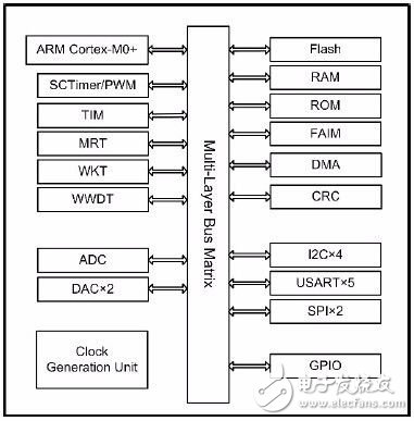
Figure 1.3 LPC84x Functional Block Diagram
The LPC84x family of MCUs is uniquely low power, with industry-leading ultra-low power performance of 90µA/MHz. Four low-power modes are supported, allowing users to select the appropriate mode based on their application needs. In the lowest power mode, the current consumption is less than 1µA.
Although these concepts may be unfamiliar to beginners, there’s no need to worry—just like how you use a computer without needing to understand its inner workings, you can still develop and program effectively with these MCUs.
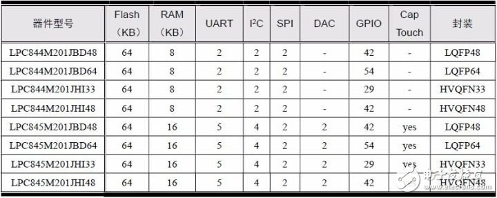
The LPC84x series MCUs come in four different packages, making them easy to choose based on specific requirements. See Table 1.3 for details.
Table 1.3 LPC84x Series MCU Selection Table
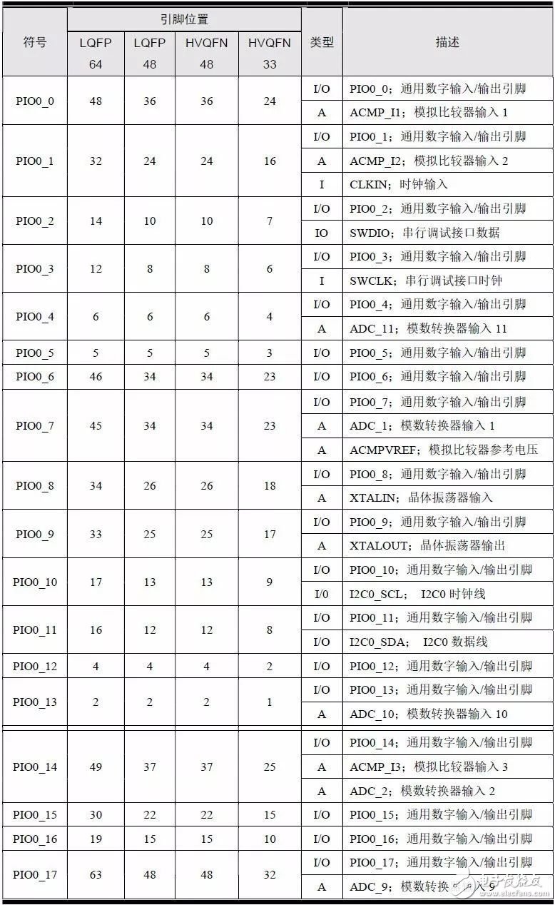
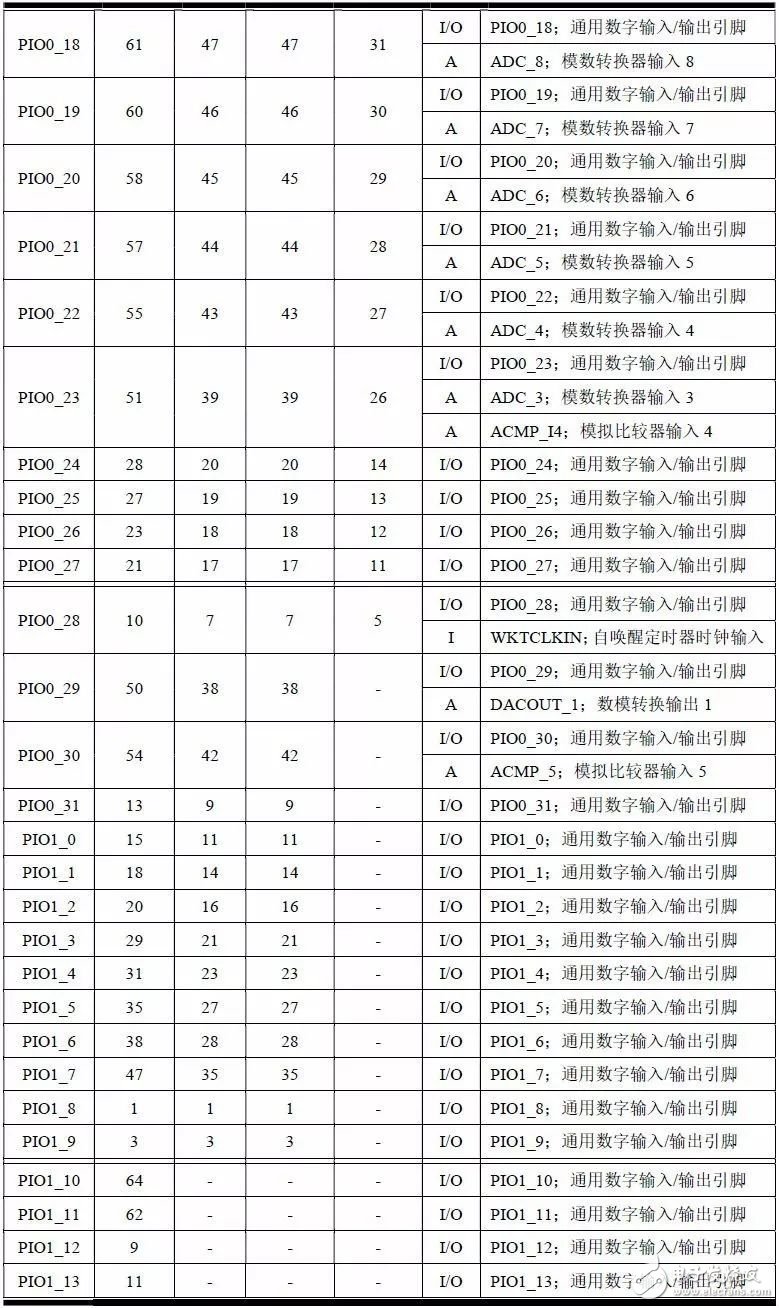
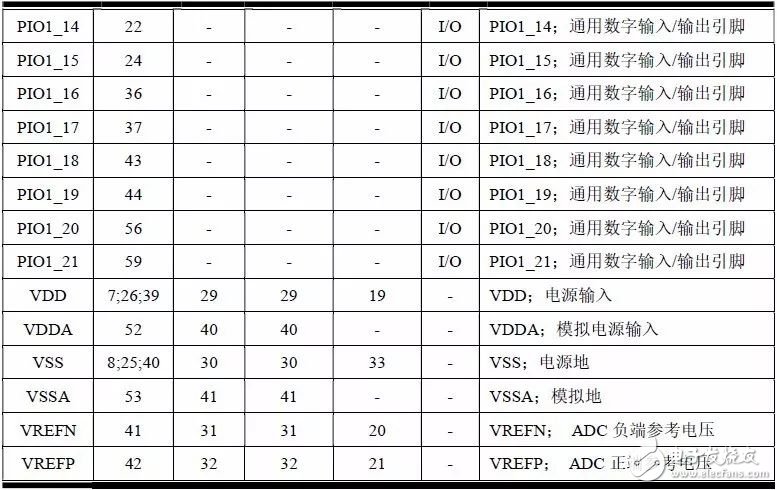
The pin descriptions and main functions of the LPC84x series MCU are shown in Table 1.4.
Table 1.4 Pin Description
best live webcam,4k pc camera,web cam 4k
Guangdong ZhiPing Touch Technology Co., Ltd. , https://www.zhipingtouch.com