Foreword
The wireless communication market such as Bluetooth® and Wi-Fi has expanded significantly, especially in the recent days where smartphones and tablets have become hubs and devices, and various AV/OA devices and home appliances for connecting smartphones and tablets. Wireless communication functions are widely installed in all devices such as wearable devices. The main communication specifications are the Bluetooth® and Wi-Fi mentioned earlier. Bluetooth® Compared with Wi-Fi, Bluetooth® is a low-speed, short-distance wireless communication technology used for transmission of small data such as voice and music data. Relative Wi-Fi is faster than Bluetooth® and can be used for long-distance communication, connecting to a residential or public network for high-capacity animation transmission.
The components of these wireless communication devices that are capable of emitting radio wave standard signals use crystal oscillators. In order to achieve high-speed, stable communication, high-precision crystal oscillators are required. The Bluetooth® and Wi-Fi standards require frequency accuracy of ±20ppm or less (frequency deviation + temperature characteristics + long-term variation). In addition, with the expansion of auxiliary equipment such as wearable devices, there is a high demand for miniaturization of mounted components, and there is an increasing demand for high-precision, small-sized crystal resonators.
This article describes the advantages, product specifications, and future trends of the best small crystal oscillator XRCGD series for clock components for wireless communications.
Advantages of the crystal oscillator XRCGD series
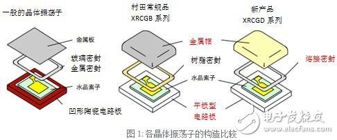
The ceramic resonator CERALOCK®, which has been supplied by Murata Manufacturing Co., Ltd. for many years, corresponds to the high-precision clock components required by the market. The small-sized, high-reliability crystal resonators developed by the company using the unique technology and developed by Tokyo Electric Wave Co., Ltd. have been in existence since 2009. Mass production began in the general livelihood market. Its biggest feature is the unique "Cap Chip" construction in the package that uses CERALOCK®'s long-term tracking record. Therefore, it has the characteristics of high productivity and supply stability, and an important characteristic of the crystal oscillator is the reduction of ESR (Equivalent Series Resistance).
If the ESR value is small, it is possible to make it easy for the IC to match the crystal oscillator when designing the circuit. Basically, the size of the ESR and the crystal oscillator are inversely proportional, so the ESR value becomes larger as the miniaturization of the crystal oscillator advances. The Cap Chip structure is a simple structure in which a metal cap is packaged on a ceramic plate. Therefore, the space utilization efficiency in the package is high, and a large crystal element can be mounted due to the size ratio of the product compared with a general crystal resonator. Therefore, the ESR value is lowered as compared with the crystal oscillator of the same size.
The crystal oscillator XRCGD series for wireless communication has a structure in which the connection portion of the metal cap and the circuit board is welded and sealed by an alloy in the structure of the Cap Chip. Therefore, compared with the company's conventional products, it realizes the characteristics of controlling the frequency temperature characteristics and long-term changes, and at the same time, it has high precision, which corresponds to the frequency accuracy pursued by the clock components for wireless communication (compared to the full frequency accuracy of the conventional product XRCGB series ± 90ppm) The XRCGD series has reached ±20ppm).
Main advantage
· With Wi-Fi and Bluetooth®, all frequency accuracy can be less than ±20ppm
· High productivity and supply stability with the same construction as CERALOCK®
· Guaranteed the same characteristics as large-sized existing crystals in a small size
· Achieved RoHS compliance, lead-free
· Corresponding to lead-free soldering installation
The general crystal resonator uses a concave ceramic circuit board, and the company uses the same flat-panel circuit board as CERALOCK®. Therefore, the space utilization inside the package is improved, and a larger crystal element can be mounted than a general crystal resonator. In addition, due to the metal cap and circuit board connection, the conventional product uses a resin package, and the XRCGD series uses a fusion package, which corresponds to the high precision of the frequency through the sealing structure. (figure 1)
XRCGD series specifications
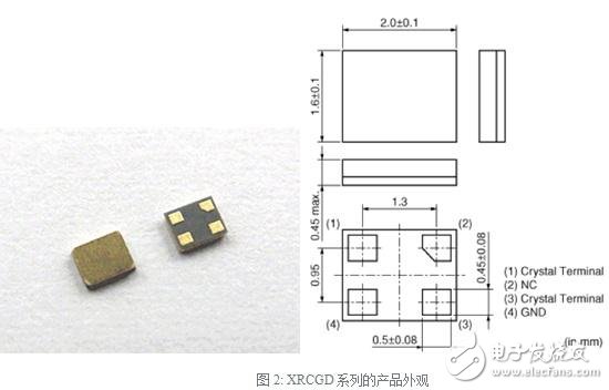
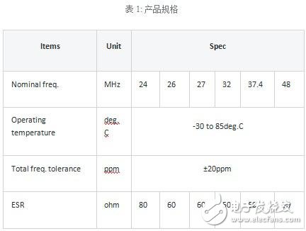
The appearance of the XRCGD series is shown in Figure 2. Product specifications are shown in Table 1. With a 2.0&TImes; 1.6mm form factor, it has achieved a 60% reduction in miniaturization compared to the current 3225 size (3.2 & TImes; 2.5mm) on the livelihood market. The corresponding frequency is superimposed on various main frequencies by wireless communication, and can correspond to a frequency widely used for a smart phone such as a smart CPU. The frequency accuracy is calculated by the initial deviation, temperature characteristics, and long-term variation, and all frequency accuracy is ±20 ppm or less. It is mainly expected to be used in high-intelligence CPUs such as Wi-Fi, Bluetooth®, and other smart phones such as smartphones and wearable devices.
Project and future prospects
The wireless communication function is not only installed in smartphones and tablets, but also in various devices such as AV/OA and home appliances. With the advancement of such devices, the density of electronic components of IC edge circuits is being formed, and miniaturization of self-setting devices such as wearable devices is also evolving. In order to meet all the requirements, our company has developed a smaller crystal resonator than the 2.0&TImes; 1.6mm size. Based on the XRCGD series, we continue to expand the product lineup of the thermistor built-in resonator and TCXO clock components. The goal is to accelerate the contribution to the high density and small size and thinness of the planned installation.
HDI PCB Specification
High density interconnect (HDI) PCBs represent one of the fastest-growing segments of the printed circuit board market. Because of its higher circuitry density, the HDI PCB design is able to incorporate finer lines and spaces, smaller vias and capture pads, and higher connection pad densities. A high density PCB features blind and buried vias and often contains microvias that are .006 in diameter or even less.
HDI PCBs are characterized by high-density attributes including laser microvias, fine lines and high performance thin materials. This increased density enables more functions per unit area. Higher technology HDI PCBs have multiple layers of copper filled stacked microvias (Advanced HDI PCBs) which creates a structure that enables even more complex interconnections. These very complex structures provide the necessary routing solutions for today's large pin-count chips utilized in mobile devices and other high technology products.
The HDI PCBs we offer include the following highly requested characteristics:
Blind and/or buried vias
Via-in-pad
Through vias from surface to surface
20 µm circuit geometries
30 µm dielectric layers
50 µm laser vias
125 µm bump pitch processing
Applications
HDI PCB is used to reduce size and weight, as well as to enhance electrical performance of the device. HDI PCB is the best alternative to high layer-count and expensive standard laminate or sequentially laminated boards. HDI incorporate blind and buried vias that help to save PCB real estate by allowing features and lines to be designed above or below them without making a connection. Many of today's fine pitch BGA and flip-chip component footprints do not allow for running traces between the BGA pads. Blind and buried vias will only connect layers requiring connections in that area.
HDI PCB
HDI PCB,Special HDI PCB,HDI Prototype PCB,HDI Board PCB
Storm Circuit Technology Ltd , https://www.stormpcb.com