Design of communication interface between CAN bus and RS-485 bus
1 Introduction of CAN bus and RS-485 bus CAN bus (Controller Area Network) is a serial data communication protocol developed by German Bosch company for automotive electronic control system in the 1980s, especially suitable for distributed control or Real-time control field. Its application range covers high-speed networks and low-cost distributed control systems. CAN has the following characteristics:
(1) Priority arbitration without destruction;
(2) Multi-master sites perform bus access according to priority;
(3) Strict error detection and definition;
(4) Support remote data request;
(5) Multi-address frame transmission by means of receive filtering;
(6) Various communication media and flexible combination methods;
(7) The data of the whole system is compatible and the system is flexible;
(8) The maximum transmission distance is 10Km (bus transmission rate is 5kbps), and the maximum transmission rate is 1Mbps (bus transmission distance is 40m).
The RS-485 standard is a serial communication protocol published by the US EIA (Electronic Industry Association). It has a longer transmission distance, faster speed and better anti-interference performance than the RS-232C standard signal, and is widely used in various industries, buildings, energy and other fields. In practical applications, many industrial control devices (such as PLC) are equipped with RS-485 interface. Therefore, it is necessary to design the communication interface circuit between CAN bus and RS-485 bus.
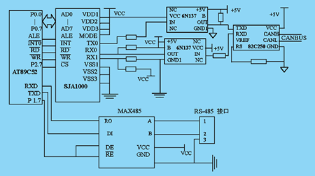
2 hardware design The entire communication interface circuit is composed of single-chip AT89C52, CAN controller SJA1000, CAN transceiver 82C250, high-speed photocoupler 6N137 and RS-485 transceiver MAX485. As shown in Figure 1. The single-chip microcomputer AT89C52 mainly completes the initialization of SJA1000 and the data communication task between CAN bus and RS-485 bus. SJA1000 is a substitute for CAN controller 82C200. It is mainly composed of the following functional modules: interface management logic, transmit buffer, receive buffer, receive filter, bit stream processor, bit timing logic and error management logic. In addition to being compatible with 82C200, it adds many new functions: PeliCAN operating mode, error counter for read / write access, reception and transmission of standard and extended structure information, programmable error limit alarm, listen-only mode, and arbitration lost interrupt . The microcontroller controls the SJA1000 internal registers by accessing external registers. The CAN transceiver 82C250 is the interface between the CAN bus controller and the physical bus, and is mainly responsible for providing the differential transmission capability to the bus and the differential reception capability to the CAN controller. Its pin 8 (RS) controls the selection of 3 different working modes: standby, slope control and high speed.
(1) Connect high level to RS, 82C250 works in low current standby mode;
(2) If RS is grounded through a connection resistor, enter the slope control mode, which can adjust the slope by changing the resistance of the resistor, which is suitable for low-speed and short bus length applications;
(3) If RS is grounded, the high-speed working mode is selected. The high-speed photocoupler 6N137 realizes the electrical isolation between the CAN controller and the transceiver, enhancing the stability and anti-interference ability of the system. RS-485 transceiver MAX485 is a differential balanced low-power transceiver, including a driver and a receiver, powered by a single + 5V power supply, specially used for TTL protocol (that is, communication protocol common to all types of CPUs) and The mutual conversion between the 485 standards allows the microcontroller to use the RS-485 serial communication protocol for direct serial communication.
The entire conversion process can be divided into: CAN bus to RS-485 bus and RS-485 bus to CAN bus. The process of converting the CAN bus to the RS-485 bus is as follows: the microcontroller receives the message sent by the CAN bus node, takes out the useful information of the message according to the data format specified by the CAN bus, and then the microcontroller sends the information to MAX485 RS-485 bus. The conversion of RS-485 bus to CAN bus is the reverse process of the above process.
3 software design The main task of software design is to realize the transmission of data and control commands between CAN bus network and RS-485 bus. It mainly includes the initialization procedure of RS-485 and CAN interface, message sending and receiving procedures, interrupt service procedures and error handling procedures. Among them, the initialization procedure of SJA1000 is a difficult point in software design, which needs to complete the setting of various working parameters. Among them, the control register is used to change the behavior of the CAN controller, including entering the reset state, activating different types of interrupt sources, such as receiving interrupts, sending interrupts, and data overflow interrupts. The acceptance code register and the acceptance mask register together define the conditions under which the message can be received by the node: the corresponding bit of the identifier of the received information is equal to the corresponding bit of the acceptance code of the acceptance code register. The role of the acceptance mask register is to determine which bits of the acceptance code are relevant or irrelevant for acceptance filtering. The bus timing register 0 defines the preset value of the baud rate and the synchronous jump width; the bus timing register 1 defines the length of the bit period, the position of the sampling point and the number of samples. The output control register can set different output modes (such as normal output mode, two-phase output mode and clock output mode, etc.). The clock divider register can not only control the output frequency of the SJA1000 and shield the CLKOUT pin, but also enable the selection of Basic CAN and Peli CAN modes. The specific SJA1000 initialization program flow is shown in Figure 2.
The procedure for converting CAN bus to RS-485 bus is as follows:
CAN-RS485_TR
ANSITION:
MOV DPTR, #SR; Status register MOVX A, @DPTR;
JNB ACC.0, CAN_QUIT;
Whether the information is received, if there is no data, exit the conversion program CAN-RS485_HANDLE:
MOV DPTR, #CANR; Receive buffer first address
MOVX A, @DPTR; The format of the received frame JNB ACC.6, RECEIVE _ FRAME
; RTR = 1, the message is a remote request frame
LCALL TRANSMIT_ DATA
; Send the data requested by the other party LJMP CAN_QUIT; Exit the conversion program RECEIVE_ FRAME: MOVX A, @DPTR;
ANL A, # 0FH;
ADD A, # 05H
; Get the length of the received data MOV R7, A
MOV R0, # 43H
; Set MCU receive data buffer DATAFRAME: MOVX A, @DPTR
; Receive data MOV @ R0, A
LCALL RS485_SEND; Forward valid information to RS-485 bus through MAX485
INC DPTR
INC R0
DJNZ R7, DATAFRAME; judge whether the reception is over RECOUT: MOV DPTR, #CMR
MOV A, # 04H
; Release receive buffer MOVX @DPTR, A
CAN_QUIT: RET; exit conversion program

4 Conclusion CAN bus is one of the most widely used field buses, and RS-485 bus is a commonly used serial bus. The mutual conversion between the two has high practical value. The CAN-RS485 communication interface circuit designed in this paper can solve the problem of mutual conversion between these two serial data buses, and has been successfully applied to an intelligent traffic control system in a certain area.
Electronic design is also trying to reduce its size while continuously improving the performance of the whole machine. From mobile phones to smart small portable products, small is always the same pursuit. High-density integration (HDI) technology enables end-product design to be more compact while meeting higher standards of electronic performance and efficiency. HDI is currently widely used in mobile phones, digital (camera) cameras, MP3, MP4, notebook computers, automotive electronics and other digital products, among which mobile phones are the most widely used. HDI boards are generally manufactured using a build-up method. The more times the layers are stacked, the higher the technical grade of the board. Ordinary HDI boards are basically one-time laminate, high-order HDI uses two or more layers of technology, and adopts advanced PCB technology such as stacking holes, plating holes, and laser direct drilling. High-end HDI boards are mainly used in 3G mobile phones, advanced digital video cameras, IC carrier boards, etc.
Pcb Hdi,Hdi Board,Hdi Pcb Design,Hdi Pcb Technology
Chuangying Electronics Co.,Ltd , https://www.cwpcb.com