Abstract: This paper introduces the basic principle and data transmission format of FSK information decoding, and uses the interface of FSK decoding chip (SM8220P) and single chip microcomputer to realize the data transmission of telephone FSK information. The related circuit diagram and program flow chart for data communication using telephone FSK information are given. Assembler source code for receiving FSK information
Telephone caller identification information transmission and reception (commonly known as Caller ID), referred to as CID (Calling IdenTIfy Delivery), is a service item provided by the telecommunication office to the called telephone user, which means that the calling telephone is displayed on the called user terminal equipment. Calling identification information such as number, calling party name, calling date and time, etc., and stored for the user to view the service items. The called user decides whether to answer the call according to the displayed caller identification information, and can avoid some unwilling to answer or unfriendly calls. With this function, the telephone network data communication for FSK information decoding can be applied to real life. 
1 Telephone caller identification principle and transmission protocol
The basic method for realizing the telephone caller identification service is that the originating program switch transmits the information such as the calling telephone number to the terminal switch through the interoffice command system, and the terminal switch then uses the frequency identification key FSK (Frequency- Shift Keying) or DualToneMulTI-Frequency mode is transmitted to the called user terminal device before the first ringing or the second ringing interval. China's communication industry standards clearly stipulate that the FSK method is used to provide the calling telephone to display the service. In a call, if the called user applies for the CID service, the terminal exchange of the telecommunication office transmits the caller identification information data to the called user. The transfer process and timing are shown in Figure 1.
Among them, A, B, C, D, and E are the state durations during data transmission, and the time values ​​of each segment are listed in Table 1. Before the data is transmitted or during the transmission, if the user picks up the phone, the transmission stops, but the call processing proceeds normally.
Table 1 CID signal transmission time value
| Symbol | Time value | Description |
| tA | 1s | First ringing signal |
| tB | 0.5s | Time interval between the end of the first ringing and the start of data transfer |
| tC | ≤2.9s | Time at which data is transmitted, including channel occupancy signals and flag signals |
| tD | ≥200ms | Time interval between the end of data transmission and the start of the second ringing |
| tE | 1s | Second ringing signal |
| tB+C+D | ≤3.6s | Each time period can be determined on a case-by-case basis |
2 Caller identification information data format
There are two transmission formats for FSK caller identification information data: Single Data Message Format (SDMF) and MMF (MulTIple Data Message Format). The former has a simple structure and can accommodate less information content, such as calling number, date and time; the latter structure is more complicated, and the length of information that can be accommodated is longer, and the name of the calling user can be selected in addition to the content of the single data format. Wait. This paper mainly introduces the reception of FSK caller information data format.
The single data message format is composed of a message header and a message body, and the message header is composed of a message type and a message length, which are both 8-bit words. The value of the message type identifies the characteristics of the message; the length of the message indicates the length of the message word followed. The message body includes messages that the switch needs to pass to the end user. The message body can hold 1 to 255 8-bit message words. Each word is represented by an 8-bit 7-bit ASCII coded character set with a check digit. 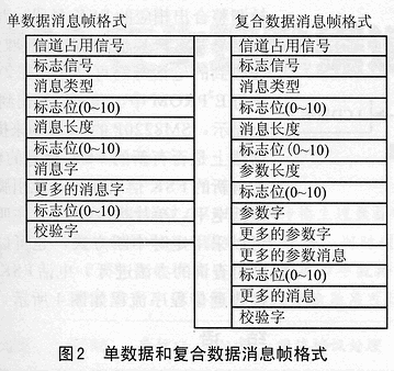
A finished message frame consists of a channel occupation signal, a flag signal, data information, and a check word. The channel occupancy signal and the flag signal are used to prompt the telephone terminal to prepare to receive data; the check word is used for error checking, as shown in FIG.
1 channel occupancy signal. This is the header flag to be sent first when the caller information is sent, consisting of a set of 300 consecutive "0"s and "1"s alternately. Its first bit is "0" and the last bit is "1". This signal is not sent during a call.
2 sign signal. In the on-hook state, the second flag signal to be sent first when the program-controlled switch sends the calling information to the user is composed of 180 flag bits (logic "1"). This signal is not sent during a call.
3 mark. The flag bit randomly inserted by the program-controlled switch according to the line usage is composed of 0 to 10 logical "1"s.
4 data words. Caller information, each data word is preceded by a “0†as the start bit, and a “1†is added as the end bit at the end, and the lowest bit of each digit is sent first. Thus, each word is actually 10 bits, ie 1PXXXXXXX0, where P is the parity bit.
When the telephone caller information data is transmitted, the channel occupancy signal is first transmitted, followed by the flag signal, and finally the data word is continuously transmitted. According to the data transmission situation, some flag bits are inserted at intervals. The general flag will be added between the following words:
a. between the message type word and the message length;
b. between the message length word and the first reference number or message word;
c. between the parameter type word and the corresponding parameter length word;
d. between the reference length word and the first reference word;
e. between the last parameter word and the next parameter type word;
f. The last reference word or message word and the check word.
Single Data Message Format Data transfer is organized into messages in the order of message type (04H), message length, message word, month, day, hour, minute, and calling number (or "O" or "P"). All message words and parameter words have odd parity bits and are transmitted in parity.
3 telephone FSK information communication circuit design
This paper takes the FSK information demodulator SM8220P chip and the single-chip microcomputer and the external circuit interface as an example to introduce the communication receiving method of FSK information. The SM8220P demodulator is a dual-in-line, low-power CMOS integrated circuit FSK demodulation chip manufactured by NPC Corporation of Japan. The pin functions of the demodulator are listed in Table 2.
Table 2 SM8220P pin function
| Symbol | Lead | Features |
| TIP-RING | 1,2 | Telephone signal input. Signal input must be DC |
| AGND | 3 | Analog ground, to be grounded through a capacitor |
| RDIN | 4 | Ring detection input. To attenuate the ringing signal and connect to this pin |
| RDRC | 5 | Ring detection RC delay circuit, active low |
| RDET | 6 | The ringing detection output is internally connected to the Schmitt trigger circuit. When it is low, it indicates that the ringing signal input is detected; when not in use, it should be grounded. |
| PWDN | 7 | Power-down control should be kept low during normal times. If it is high, enter power-down mode, COSCOUT, CDET and DOUT are automatically set to high level, AGND, FOUT are set to high impedance state |
| GND | 8 | Device ground |
| OSCIN/CLKIN | 9 | Oscillator amplifier input, external oscillator input signal is input through this pin |
| OSCOUT | 10 | Oscillator amplifier output, must be open when using external oscillating signal |
| CDET | 11 | Carrier detect output, active low. When it is low, it indicates that there is FSK carrier signal input at this time. |
| NC | 12 | Empty foot |
| DOUT | 13 | Data output, usually high level. When CDET=0, it indicates that there is a valid FSK signal input on the phone, and it is output by the pin after demodulation. |
| DMIN | 14 | Demodulator input |
| FOUT | 15 | FSK bandpass filter output connected to DMIN via a capacitive coupling |
| VDD | 16 | Positive power supply (3~5.5V) |
The SM8220P follows the Bell 202 and ITU-T V.23 protocol standards and is transmitted as a continuous binary pulse frequency shift keying signal at a transmission rate of 1200 bps. Support FSK number display and name display and other functions; the chip contains power supply power failure detection circuit, ringing detection circuit and carrier detection circuit; signal input detection sensitivity is high, power supply operating voltage is wide (3 ~ 5.5V), is carried out A better integrated chip for telephone FSK information decoding communication.
In order to realize the reception of the telephone FSK information, the P87LPC764 single-chip microcomputer is used to control the SM8220P circuit to complete the work of the telephone FSK information decoding communication. The specific circuit of telephone FK information communication is shown in Figure 3.
As can be seen from Figure 3, for FSK signals transmitted from the telephone line, the signal is transmitted between the first ringing and the second ringing. The ringing signal is rectified and divided, and is applied to the transmitting tube of the TIL113 photoelectric coupling device, so that the transmitting tube has a current passing through and emits light, and irradiates the base of the phototransistor to make the phototransistor saturate and conduct. A pulse signal greater than 1V is obtained on R6, and input to the external interrupt 0 of the MCU to wake up the MCU to receive. After 0.5s, the FSK signal is separated and attenuated by C3, C4, R1, C2, input to the differential input terminals TIP and RING of the FSK receiver SM8220P, and the FSK signal is read and demodulated and the ASCII code string is output from the DOUT pin. The line sequence is received and processed by the P87LPC764 MCU, and the corresponding phone FSK information is extracted and sent to the multi-function LED display module MAX7219 to drive the digital display and 24C64 to save.
4 FSK information receiving communication software design
The recognition process of the ASCII serial sequence of the SM8220P output by the single-chip microcomputer consists of two parts: reception and data integration. Since the baud rate of the FSK signal is 1200 bps, the time per bit is 833 us. Therefore, it is possible to set the timer to receive 1 bit per 833 us and 1 number for every 10 bits. This loops repeatedly until full FSK information is received. When there is a call, after the first ringing, the MCU starts to detect the received signal, and the SM8220P starts to receive 300 channel occupation signals consisting of 0 and 1 with a frequency of 1200 Hz and 180 “1†flag signals, followed by Receive the calling number and time. Each time a number is received, the SM8220P converts it into a 10-bit (1PXXXXXXXX0) serial sequence, which is transmitted from the 13-pin output to the P87LPC764 microcontroller. The P87LPC764 integrates the detection with the corresponding FSK number, time, etc. through precise timing programming. Data, complete FSK information decoding, receiving communication, received phone number can be saved in 24C64 serial E2PROM, can also be output to LCD display. The 11 pin of the SM8220P is used to indicate whether there is new FSK information input on the telephone line. This pin will generate a low level if there is a new FSK information input. The MCU receives the FSK caller information by using the timed interrupt mode or by using the delayed query method. The flow of the telephone FSK information receiving communication program is shown in FIG. 4.
Conclusion
In recent years, China's telecommunications network infrastructure has developed rapidly, and the telephone penetration rate has increased year by year. According to the survey, users urgently need to use the phone to deliver more information. By using the combination of SM8220P and single-chip microcomputer, it is convenient to realize the decoding and receiving communication of telephone FSK information, and realize the functions of remote automatic meter reading by users using telephone network.
Note: See the website for the decoding of the FSK information and the assembly of the receiving communication.
Ferrite Ring Magnets, Permanent Ring Magnets.Y25 Ferrite Magnet Ring
HU NAN YUBANG MAGNETIC MATERIAL CO.,LTD , https://www.ybmagnet.com