ITO and what is the relationship?
ITO is a transparent electrode material with high electrical conductivity, high visible light transmittance, high mechanical hardness and good chemical stability. At present, the ITO film is mainly for improving the light extraction efficiency of the LED.
What is the Burstein-Moss effect?
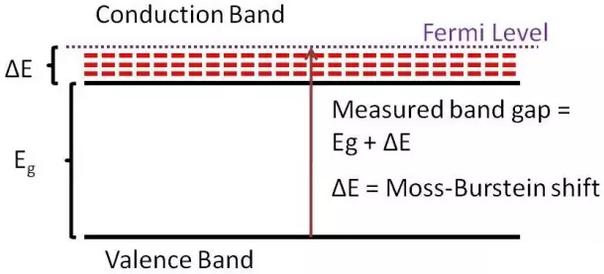
Burstein-Moss effect: When the semiconductor is heavily doped, the Fermi level enters the conduction band, and the intrinsic light absorbs the edge toward the high energy direction.
In a commonly doped semiconductor, the Fermi level is between the conduction band and the valence band. When the n-type doping concentration rises, the Fermi level is slowly pushed into the conduction band due to the accumulation of electrons in the conduction band (it can be easily understood as the water to which the ice (Fermi level) is increased ( Electronic) pushed to the high position).
What is a precursor?
Precursors refer to specially treated mating materials used to synthesize and prepare other materials.
Recently, researchers at Sun Yat-sen University invented a process for preparing indium tin oxide film (ITO) in LED structures by metal organic vapor phase deposition (MOCVD), which can effectively enhance the transparent conductive properties of UV LEDs.
Generally, UV LEDs are classified into three types according to wavelength: UVA UVB UVC. At present, it is mainly used in the fields of water purification, biological sterilization, medical diagnosis and treatment, and ultraviolet treatment.
research process
Although ITO is a transparent conductive layer material in the visible spectrum region, the transparency of ITO is gradually reduced in the ultraviolet region.
Therefore, the Sun Yat-Sen University team managed to extend the width of the optical band gap to 4.7 eV using MOCVD technology. The forbidden band excites the photon wavelength just in the ultraviolet region (364 nm).
Generally, UV LEDs are classified into three types according to wavelength: UVA UVB UVC. At present, it is mainly used in the fields of water purification, biological sterilization, medical diagnosis and treatment, and ultraviolet treatment.
Fig.1 Photoelectric characteristics of ITO film in 90nm MOCVD process
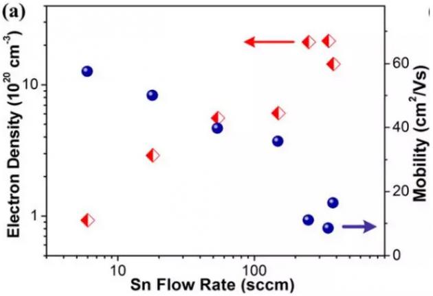
(a) Effect of Sn flow rate on electron density and mobility
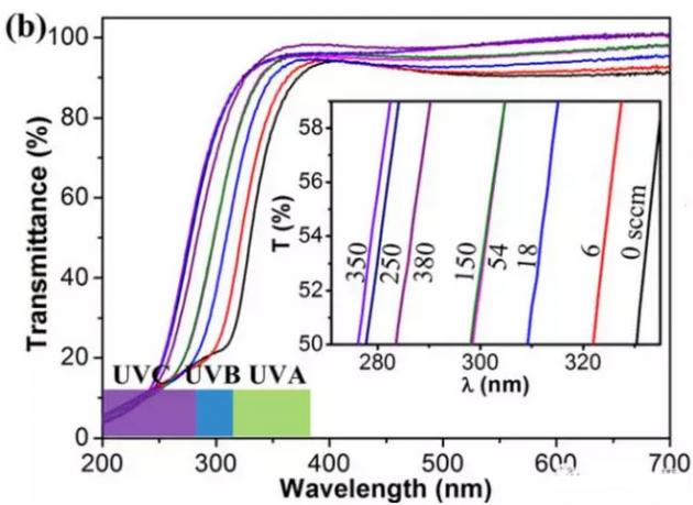
(b) UV visible light transmittance and different tin flow rates in the ITO film of the MOCVD process.
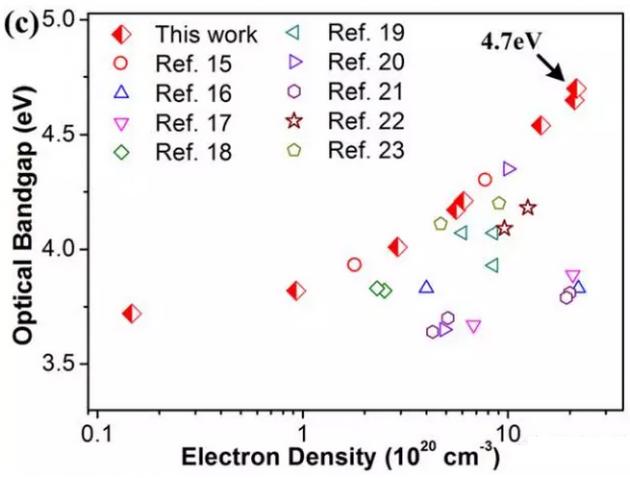
(c) Comparison of ITO optical forbidden bands under different processes
The Sun Yat-Sen University team first used the MOCVD technique (the growth environment temperature was about 500 °C) to grow a 90 nm ITO film on the surface of the sapphire. The precursors were trimethyl indium, tetrakis-dimethylamino tin, and oxygen. Argon mixed gas. The resulting material surface is attached with particles of a pyramid-like shape (100) and a triangular shape (111).
After many research experiments, the researchers found that the rate of addition of the precursor to 350 cubic centimeters per minute would reach the highest free electron density (2.15x10²¹/cm3). At the same time, the optical band gap will reach 4.70eV. Usually, indium oxide (In2O3 has no precursor) has an electron density of only 1.47 x 10¹⁹/cm3 and a forbidden band width of 3.72 eV.
The difference in the forbidden band width is mainly due to the effect of the Burstein-Moss effect, in which some free electrons are concentrated in the lower conduction band, so more photon energy is needed to excite electrons from the valence band. come out. The researchers said that using this method to widen the forbidden band width by 0.98 eV, this increase of close to 1 eV is rare.
At the same time, the researchers also believe that the MOCVD process can improve the lattice distortion problem (lattice distortion), which is one of the reasons for the narrow band gap of ITO.
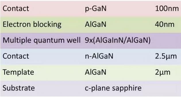
Figure 2 Extension structure of the LED
Generally, a magnetron sputtering process can also produce a 120 nm light-transmissive conductive layer compared to the MOCVD process. This process uses a mixture of tin oxide (SnO2) and indium oxide (In2O3) with a composition ratio of 1:9. The magnetron sputtered material was annealed at 550 ° C and placed in a nitrogen atmosphere for 5 minutes.
By analyzing the spectrum, the peak wavelength of the UV LED at this time was 368 nm (Fig. 3a). At this wavelength, the transmittance of the ITO film in the magnetron sputtering process was 86%, and the transmittance of the ITO film in the MOCVD process was 95%. However, the resistivity of the ITO film in the magnetron sputtering process is smaller than that of the ITO film using the MOCVD process, and the contact resistance of the magnetron sputtering process is larger.
Fig. 3 Photoelectric characteristics of 120nm MOCVD ITO film and magnetron sputtered ITO film
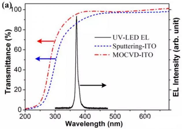
(a) Conductivity of 120 nm MOCVD ITO film and magnetron sputtered ITO film on sapphire substrate, and LED luminescence spectrum using MOCVD ITO film
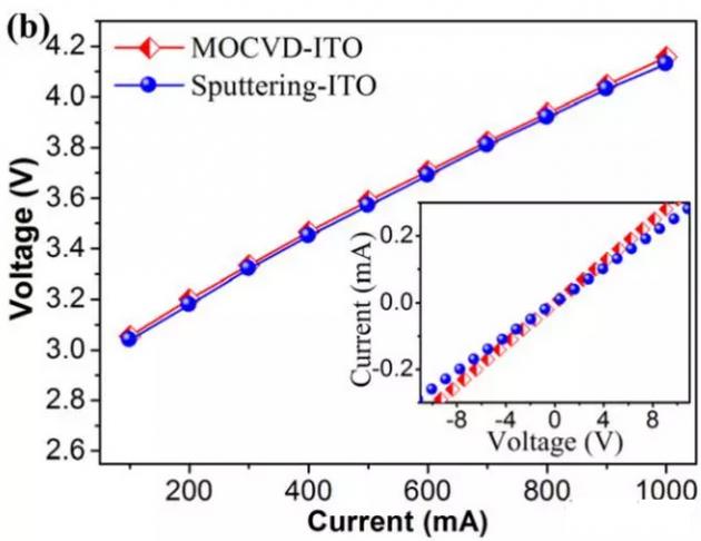
(b) LED current-voltage characteristic curve of ITO film using two processes
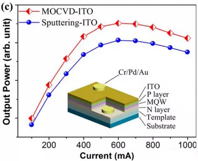
(c) Characteristic curve of output power and current
in conclusion
The CVD film of the MOCVD process can increase the output power by 11.4% and 14.8% at currents of 350 mA and 600 mA, respectively (Fig. 3c). After multiple sample tests, the average operating voltage was 3.45V at 350mA operating current. The LED current-voltage curves of the ITO films using the above two processes are almost identical (Fig. 3b).
references
Chen, Z. , Zhuo, Y. , Tu, W. , Ma, X. , Pei, Y. , Wang, C. , & Wang, G. (2017). Highly ultraviolet transparent textured indium tin oxide thin films and the application in light emitting diodes. Applied Physics Letters, 110(24), 242101. Https://doi. Org/10.1063/1.4986452

AC wall 5V 2A power adapter with multiple tips works for many small 5V electronics. Like Scanner, Router, Bluetooth speaker, Foscam Wireless IP Camera, CCTV camera, USB hub, bluetooth GPS Receiver, tv box, tablets, Baby Monitor, Graco Swing, Home Phone System, VoIP Telephone Routers, Serato DJ Controller, DVR, ADSL Cat, External battery, hubs, switches, Led Strip, String Lights, vibrator, Raspberry pi 3 Raspberry Pi A/A+/B/B+ Raspberry Pi Zero and more 5V devices. (5V ONLY)
Worldwide Input: 110-240V; Output: 5V 1000mA, 1.5A, 1.75A, 5V 1A, 5V 500mA, 5V 2.1A, Max 10W. DC Tip Polarity: Central Positive(+). Please read manual carefully before using 5vdc power supply.
Design-safeguard features against incorrect voltage, short circuit, internal overheating and overloading. This 5v Ac power supply charger is made from quality material to ensure the long lifetime. Power your 5v electronics perfectly and replaces lots of 5 volt power chargers
Package include: 1 x High Quality 5V 2A AC DC Power Adapter, 1 Set x Tips
5V Switching wall charger 6V Switching wall charger 9V Switching wall charger 12V Switching wall charger 15V Switching wall charger 19V Switching wall charger 24V Switching wall charger 36V Switching wall charger 48V Switching wall charger
Shenzhen Waweis Technology Co., Ltd. , https://www.waweis.com