I. Introduction
This scheme is a determinant matrix keyboard interface circuit based on RS232 bit serial communication bus realized by VHDL language. It has reset and serial data receiving and transmitting functions. According to the display state of LED led0-led2, the chip can be judged. The working conditions; the program to realize all the circuit functions is debugged on the EPM7128SLC84-15 chip with field programmable function produced by ALTERA Company in the United States. The dynamic scanning can be used to determine the key press, convert the key value into the corresponding ASCII code value, and realize the reception and transmission of the serial data by the action of the clock pulse.
Second, the design plan
1. Chip pin definition
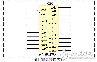
Reset reset input; clk clock input; rxd serial data receiver; retn0-retn7 keyboard scan line input line; txd serial data transmitter; scan0-scan7 keyboard scan column output line; led0-led2 display output.
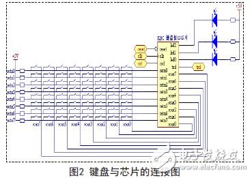
2. Keyboard and chip connection diagram (as shown in Figure 2, 8 & TImes; 8 64-key keyboard)
3. Dynamic scanning principle
(1) The column lines scan0-scan7 are sequentially output to the 0 level, and the level state of the row lines retn0-retn7 is checked. If the level of the line line retn0-retn7 is all high level, it means that no key is pressed. If the level on retn0-retn7 is not all high, it means that there is a key press.
(2) If no key is pressed, it will return to scanning. When a key is pressed, a progressive scan is performed to find the key number of the closed key. The process is: first scan0=0, scan1-scan7=1, detect the level on retn0-retn7, if retn=0, it means that the first column of the first row is pressed, if retn1=0, then The key indicating the second row and the second column is pressed, and the others are analogous; if retn0-retn7 is not 0, it means that the column is not pressed; then scan1 is detected, and the second column is detected. Loop down and know to find the closed key.
When a key is pressed, it is possible to determine which key is pressed based on the scan value and the rent value at that time.
4. Chip internal module block diagram
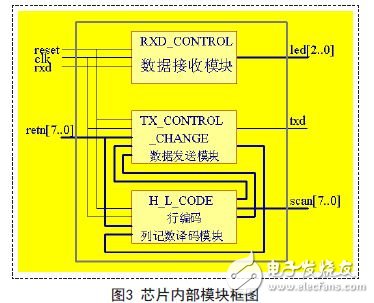
Third, chip design
The block diagram of the data receiving module is shown in Figure 4.
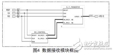
Reset reset input; clk clock input; rxd serial data receiving end; led[20] outputs the lower three digits of the ASCII code value corresponding to the key to drive the LED.
This module implements the control function of receiving count and serial-to-parallel conversion of serial data.
1. Serial data receiving control unit
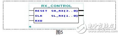
Reset reset input; clk clock input; rxd serial data receive; sh_rx[30] receive counter high 4 bits; sl_rx[10] receive counter low 2 bits.
Set the serial data receive counter to a 6-bit counter. The upper 4 bits are sh_r and the lower 2 bits are sl_r. The status of the counter is used to implement synchronous control and count control of serial data.
2. Serial-to-parallel conversion circuit unit
After the serial data received from the RXD terminal is serially converted, the lower three bits are output through the LED output terminal, and the LEDs LED0, LED1, and LED2 are driven to emit light, thereby displaying the lower three bits of each data of the receiving end RXD. When the lower three bits of each data are the same, the display state does not change, otherwise flickering occurs to check the operation of the chip.
Fourth, summary
This scheme is a design of determinant matrix keyboard interface circuit based on RS232 bit serial communication bus realized by VHDL language. It has reset and serial data receiving and transmitting functions. It can be judged according to the display state of LED led0-led2. The operation of the chip; the program to realize all the circuit functions is debugged on the EPM7128SLC84-15 chip with field programmable function produced by ALTERA Company in the United States. The design of the circuit is close to life and practical, and can be used as an interface between a general PC keyboard and a host after being fabricated into a chip.
Network Cabinet is widely used for 19 inch network server enclosure perferated cabinet installing and placing of 19" international standard equipment and the system integration. Network Cabinets support large, modular network switches by providing additional space for cable management and side-to-side airflow solutions.
Network Cabinet
Network Cabinet,Electrical Cabinets,Wall Mount Server Cabinet,Wall Mount Server Cabinet,Wall Mount Cabinets,Electrical Distribution Cabinets
Sijee Optical Communication Technology Co.,Ltd , https://www.sijee-optical.com