1. System overall plan
1.1 Overall design block diagram
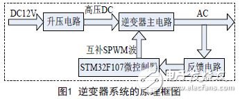
As shown in Figure 1, the inverter system consists of a boost circuit, an inverter circuit, a control circuit, and a feedback circuit. The DC12V of the low-voltage DC power supply is boosted, rectified and filtered by the booster circuit to obtain about DC170V high-voltage direct current, and then filtered by the DC/AC conversion and LC filter of the full-bridge inverter circuit to obtain AC110V sinusoidal alternating current.
The inverter uses the ARM controller as the control core. The feedback signal of the output voltage and current is processed by the feedback circuit and then enters the on-chip AD of the ARM processor. After the AD conversion and the digital PI operation, the corresponding SPWM pulse signal is generated, and the SPWM is changed. The modulation ratio can change the output voltage to complete the closed-loop control of the entire inverter.
1.2 SPWM solution selection
1.2.1 PWM power chip solution
Using ordinary PWM power control chips, such as SG3525, TL494, KA7500, etc., the advantage of such chips is that they can directly generate pulse width modulation signals, but its disadvantage is that the waveform is not linear, and the oscillator generator relies on the charge and discharge circuit. To generate a waveform, an additional extra circuit is required when the PWM chip is to generate the SPWM signal.
1.2.2 CPU software solution
The CPU generates SPWM pulses, such as single-chip microcomputer, ARM or DSP. The advantage of this method is that the pulse width can be adjusted by software, which not only has high precision, but also the peripheral circuit is very simple and cheap.
Finally, the STM32F107 (ARM) is selected to complete the generation of the SPWM pulse and the control of the entire inverter.
2. System hardware circuit design
2.1 CPU controller
The CPU is the core part of the whole inverter, and is mainly responsible for the acquisition of feedback signals, digital PI closed-loop calculation, PWM wave output, parameter setting and external communication. The CPU adopts ST's latest STM32F107 series ARM chip. This series of chips uses ARM's 32-bit Cortex M3 as the core, and the highest frequency is 72MHz. The Cortex core has a single-cycle hardware multiplication and division unit, so it is suitable for high-speed data processing. The chip features three independent conversion cycles, a low-speed 1μs high-speed analog-to-digital converter, and three independent digital-to-analog converters with separate sample-and-hold circuits, making them ideal for three-phase motor control, digital power, and networking applications. The chip also has a rich communication unit, including an Ethernet interface, five asynchronous serial interfaces, a USB slave device, a CAN device, I2C and SPI modules.
2.2 Drive and inverter circuit
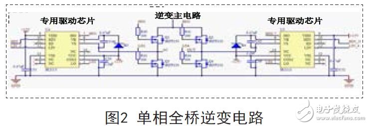
The inverter main circuit uses a single-phase full-bridge inverter circuit based on the H-bridge as shown in Fig. 2. The single-phase full-bridge inverter circuit is mainly composed of four MOSFETs Q1, Q2, Q3 and Q4. If the load is added between AC and OUT, the inverter circuit is formed. Controlling Q1, Q2, Q3, and Q4 is turned on and off in a certain order to obtain a desired sinusoidal waveform.
For this design, the choice of switching tube is mainly based on its rated voltage and rated current. Here, the IRFP460N channel-enhanced MOS transistor with a rated voltage of 500V and a rated current of 20A is selected as the switching tube. Can meet the design requirements. In order to limit the drive current of the MOSFET gate, a series current limiting resistor is required in the gate to prevent device damage caused by overcurrent.
2.3 Filter circuit
The voltage waveform generated by the two SPWM signals on the load resistor is a square wave that changes according to a sinusoidal law. It is a bipolar SPWM waveform. What is actually needed is a sine wave with a frequency of 50 Hz, so the SPWM wave needs to be filtered. A typical PWM inverter uses an LC low pass filter. For the design of the LC filter, first consider the cutoff frequency of the filter. The cutoff frequency of the LC filter is shown in equation (1).
![]()
Considering the harmonic distortion of the output voltage of the filter, the dynamic response of the system, and the factors such as volume and weight, the cutoff frequency is selected and selected.
Coupletech Co., Ltd could manufacture and supply a variety of nolinear Optical Crystal ( NLO crysal ), which is Lithium Triborate (LBO) crystal, Potassium Titanyl Phosphatecrystal ( KTP ) crystal, KTA crystal, Beta Barium Borate ( BBO) crystal, BIBO crystal, Lithium niobate ( LiNbO3, LN ) crystal, Potassium Dihydrogen Phosphate & Potassium Dideuterium Phosphate (DKDP (KD*P) and KDP ) crystal, periodically poled crystal ( MgO: PPLN, PPLN ) crystal and infrared Nonlinear Optical Crystals ( AgGaS2, ZnGeP2 ) crystal with top quality, unbeatable prices, prompt delivery and the best pre- and post- sales technical support and services, for not only science users but commercial customers and industrial manufacturers all over the world.
Coupletech's NLO crystal is widely used for frequency doubling ( SHG ), third-harmonic generation ( THG ), sum frequency (SFG), optical difference frequency ( DFG ), optical parametric oscillator ( OPO ), and so on.


Nonlinear Optical Crystals,KTP Crystals,BBO Crystals,LBO Crystals,BIBO Crystals,KTA Crystals,LN Crystals,PPLN Crystals
Coupletech Co., Ltd. , https://www.coupletech.com