Abstract: This paper introduces the principle and application of Sanken's hybrid Switching Power Supply ICSTRF6600 series. As an example, it introduces the design of a 34′′ color TV switching power supply using STRF6656, and gives satisfactory experimental results.
1 Introduction
This article refers to the address: http://
Hybrid power ICSTR-F6600 series is a product of Sanken Electric Co., Ltd. in Japan in recent years. It contains MOSFET and control IC part, which is specially designed for flyback converter, especially suitable for color TV switching power supply.
The hybrid IC can operate in a quasi-resonant mode and a pulse duty cycle control (PRC-PulseRatioControl) mode. It features the second-generation SMPSIC, which features secondary output sampling and optocoupler feedback regulation, quasi-resonance, high efficiency, wide input range, good input voltage regulation and load output characteristics, as well as overcurrent and overcurrent. Pressure and thermal protection, etc. Compared with other manufacturers of the same type, it has one more thermal protection and less electrical noise of the switch, which can simplify or even eliminate the surge absorbing circuit.
This paper introduces the working principle of this series of ICs. On this basis, it describes how to design and manufacture a 34′′ color TV switching power supply. The prototype power supply circuit, transformer design and experimental results are given. Experiments show that the power supply is completely compatible with the TV set. Electrical requirements, it has few external components, easy design and high stability. It meets national standards in environmental and safety experiments such as high temperature, low temperature, EMI, short circuit and open circuit. It is a rare and high-performance TV practical. Switching power supply.
2 Hybrid Switching Power Supply Controller STR-F6600 Series Principles and Features
Figure 1 shows the block diagram of the STR-F6600 series. This is a plastic packaged IC with a pinout. The function of each foot is shown in Table 1.
Table 1 STR-F6600 series per foot function
| Pin | symbol | Description | Features |
|---|---|---|---|
| 1 | OCP/FB | Overcurrent/Feedbackterminal | Output overcurrent detection signal and regulation control signal |
| 2 | S | Sourceterminal | MOSFET source |
| 3 | D | Drainterminal | MOSFET drain |
| 4 | VIN | Supplyterminal | Power input of the control circuit |
| 5 | GND | Groundterminal | Ground |
2î€1 start circuit
When the AC power supply is added at t0, it can be seen from Fig. 2 that in a half cycle, the peak-to-ground voltage VA≈Vd (rectified voltage) from point A, VA is charged to C909 through R902, so that the voltage Vin on IC pin 4 rises approximately linearly. (See Figure 3). When Vin rises to the threshold voltage Vin(ON)=16V
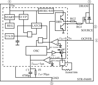
Figure 1 STR-F6600 series block diagram
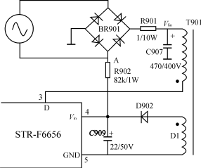
Figure 2 starting circuit
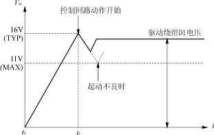
Figure 3 waveform of the Vin port voltage at startup
When the control circuit in the IC starts, the input current Iin on the Vin port rises from 100μA to 30mA, and the capacitor C909 does not have enough power to make Vin fall. If the DC voltage supplied by the drive winding D1 is sufficient at this time, Vin will not fall below the threshold of 11V, and the IC continues to operate successfully. The number of turns of the drive winding D1 shall be such that after rectification, the voltage on C909 exceeds 11V and is also lower than 20.5V. The overvoltage protection circuit works because Vin is greater than 20.5V, and the undervoltage protection circuit works when Vin is less than 10V. Generally, it is more suitable to take 18V from Vin.
The selection of R902 and C909 should be appropriate. If R902 and C909 are too large, the IC startup time t1t0 will be prolonged. However, the C909 can't be too small, otherwise it can't maintain the IC action until the drive winding voltage arrives, so it can't start smoothly. Generally, the wide power supply (90-270) VAC voltage C909 takes (47 ~ 100) μF, R902 takes 47kΩ ~ 68kΩ is suitable, for narrow power supply (200VAC), R902 can take 82k ~ 150k. In this example, when R902=82kΩ, C909=47μF, and the input voltage is 90V, the startup time is about 1.3μs.
2î€2 internal oscillator, voltage regulation principle and overcurrent protection
(1) Internal oscillator
The internal oscillator of the IC forms an oscillation pulse by charging and discharging C1, and the discharge time constant C1R1 (≈50μs) determines the off time of the MOSFET. In the PRC mode of operation, the regulation is achieved by a fixed toff and a change of ton. Figure 4 shows the operating waveform of the internal oscillator when there is no regulated control signal input. As can be seen from the waveform of Figure 5, capacitor C1 is charged to 6.5V when the MOSFET is turned on. At the same time, the drain current ID is gradually increased, and a sawtooth shape voltage VR5 is formed on R5. VR5 is added to the IC's 1-pin OCP/FB port with almost no loss after R4. When the 1-pin voltage V1 reaches the threshold Vth1 ≈ 0.73V, the comparator 1 starts to operate, which inverts the oscillator output and turns off the MOSFET through the driver stage. Thereafter, C1 is discharged through the resistor R1, and the voltage across C1 linearly decreases with a constant discharge time constant C1R1. When it drops to around 3.7V, the oscillator output is inverted again, causing the MOSFET to turn back on, and the C1 voltage jumps again to 6.5V. This process is repeated continuously.
As can be seen from the above, the on-duration ton of the MOSFET is determined by the rising slope of VR5, and toff is determined by C1R1 in the PRC mode.
(2) Principle of voltage regulation
As shown in Figure 5, in order to control the output, the error signal of the optocoupler
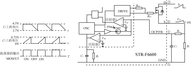
Figure 4: Oscillation waveform when no regulated control signal is input.
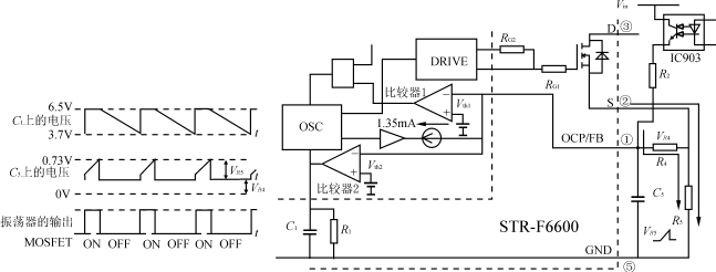
Figure 5 shows the oscillating waveform under the action of the regulated control signal.
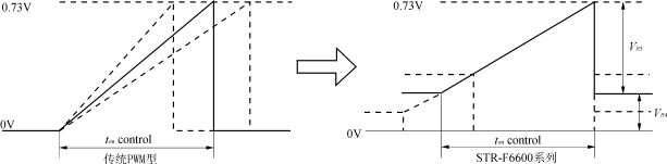
Figure 6 V1 waveform during conduction
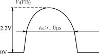
Figure 9 quasi-resonant signal during the cutoff period
The output current forms a voltage drop VR4 on R4 in series with VR5, so that the waveform part of the voltage V1 input to pin 1 is controlled by VR4, so that comparator 1 is inverted or delayed, to change the ton of the MOSFET to change The secondary output voltage achieves the purpose of voltage regulation. This is a current control method. In general, in the current control mode, VR4 rises at light load, and it is possible that the noise caused by the inrush current when the MOSFET is turned on causes false triggering to the comparator 1. To solve this problem, an active low-pass filter is inserted during the turn-off of the MOSFET. It consists of a C5 and a 1.35mA constant current source, connected between pin 1 and ground. Before the MOSFET is turned on, the filter shunts about half of the current output from the optocoupler, thus effectively reducing the VR4 DC offset, preventing false triggering caused by the superposition of the inrush current, and the presence of C5. It also increases the absorption bypass effect on noise.
It should be noted that the control of ton is now achieved by changing the DC voltage of VR4 (see Figure 6). This is different from the traditional methods in the past. The past STR-S6700 and STR-M6800 series changed by changing the slope of the charging voltage. Ton.
(3) Overcurrent protection
This is an overcurrent detection circuit with pulses connected to the pulse. As can be seen from the waveform in Figure 5, the comparator 1 acts as an overcurrent protection. As long as the voltage V1 peak proportional to Id exceeds the limit of 0.73V, the oscillator output is forced to be inverted, the MOSFET is turned off, and ton becomes smaller, achieving the purpose of limiting the output current and output power.
2î€3 quasi-resonant application
The PRC operation of the pure optocoupler feedback circuit is discussed above. The actual application circuit should include the feedback branch from the transformer drive winding D1 (which includes D903, R908, C913, D904, etc.) due to the existence of this branch. Therefore, V1 contains a voltage component proportional to VDS during the turn-off of the MOSFET, which is called a quasi-resonant signal (see Figure 7). According to the level of the quasi-resonant signal, it can be determined whether the power source operates in the PRC mode or the quasi-resonant mode.
If the quasi-resonant signal V1 is between 0.73V and 1.45V during MOSFET turn-off, comparator 1 acts to bring the power supply into PRC mode; if quasi-resonant signal V1 exceeds 1.45V (V1 maximum is 6.0V), then Comparator 2 acts to reduce toff to about 1.5 μs (min), but the current off time of the power tube does not depend on this value, but is much larger than it. In fact, as long as V1 remains greater than 0.73V, the MOSFET remains off and when it begins to turn on, it is determined by the quasi-resonant mode. The quasi-resonant mode is to make the MOSFET turn on at half a cycle of the VDS resonant period, which can ensure lower switching electrical stress and reduce switching loss. To achieve this, the following two conditions must be met:
(1) There is a suitable capacitor C908 between the drain and the ground, which forms an LC resonant circuit with the primary inductor to form a resonant waveform of the voltage VDS between the drain and the source;
(2) There must be a suitable delay in the gate drive to ensure that when the quasi-resonant signal V1 falls below 0.73V, the MOSFET begins to conduct exactly at the lowest point of the VDS waveform. In the specific adjustment, a power meter can be used to monitor the power input terminal. Under a fixed output load, the R908 and C913 sizes can be adjusted to obtain the minimum input power. At this time, the delay time can be judged to be the most suitable. It should also be noted that the delay also has the involvement of the C910 and the circuit's distributed capacitance, so even without the C913, the circuit will have some delay.
2î€4 drive circuit, lock trigger, thermal protection and overvoltage protection
(1) Drive circuit
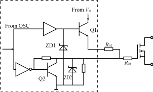
The drive circuit is shown in Figure 8.
This is a constant voltage drive circuit that uses a Zener diode ZD1 (8.6V) to protect the constant drive signal amplitude. When the drive signal is a positive pulse, Q1 is turned on, and the MOSFET is excited by the resistor RG1+RG2 to become a soft switch. When the input signal is at zero level, Q1 is turned off, Q2 is turned on, and the MOSFET gate charge is rapidly discharged through a small resistor RG1. The function of Zener diode ZD1 is to protect the MOSFET from being damaged by the VDS (500V ~ 600V) that is not overshooted by the D-G inter-electrode coupling to the gate.
(2) lock trigger Latch
When the circuit overvoltage or overheat occurs, the relevant circuit in the chip will turn ON the lock flip-flop, so that the voltage Vin on the 4 pin swings back and forth between 10V and 16V. The IC works intermittently, preventing abnormal rises in current and voltage until the Vin is below 6.5V and the circuit is completely unstimulated. At this time, if you want to restart the power supply, you need to turn it off and then turn it on.
(3) Thermal protection circuit
When the case temperature of the hybrid IC exceeds 140 °C, the thermal protection circuit in the control IC will activate the lock flip-flop to turn ON, because the MOSFET and the control IC are mounted on the same substrate. So thermal protection also includes MOSFETs.
(4) Overvoltage protection circuit
When Vin exceeds 22.0V, the overvoltage protection circuit can activate the trigger locker. The Vin will swing back and forth between 10V and 16V and will eventually drop below 6.5V. The power supply will stop working completely. At this time, it must be turned off and then turned on to restart.
The overvoltage protection circuit also prevents the secondary output voltage VO1 from being too high. For example, when the control circuit is open or the VO1 is greatly increased due to other reasons, the induced voltage of the driving winding is also increased by the transformer coupling, so that Vin is raised. Overvoltage protection also works when Vin exceeds 22V. Limiting the re-elevation of VO1, the VO1 at this time is ![]() VO1(OVP)=
VO1(OVP)=
For example, if VO1 (normal value) = 130V and Vin (normal value) = 18V, VO1 (OVP) = 162.5V can be calculated by the above equation, which means that when the fault occurs, the VO1 will not exceed the maximum due to the overvoltage protection. This value.
3 adjustment and test results
Three 34-inch color TV prototypes were installed using the above power supply. When the power was first turned on, the power supply did not work. Then the oscilloscope was used to observe the Vin waveform. It was found that the voltage was too low, so the drive winding ND1 was changed from 4Ts to 5Ts, and the Vin was too large. The vibration is extinguished once and again (because of the overvoltage protection), then a series resistor of 10Ω/1W is added to the branch of the rectifier diode D904. The problem is solved. When the Vin is stable, it reaches 17V and can be turned on smoothly.
In debugging, in order to get the best quasi-resonant working state, you can connect an AC power meter to the power line end of the TV, input 264V AC, and adjust the picture to black field, turn off the sound (this time switch The power supply has the highest oscillation frequency. In this case, the parameters of the delay circuit components R908 and C910 are adjusted until the reading of the power meter Pi is minimum. At this time, the switching loss of the power supply is minimum, and the circuit operates in the optimal quasi-resonant mode.
Experiments show that the power switch has less noise interference and can easily pass the EMC test without adding special anti-interference measures. However, in the steady-state STANDBY state, the input power consumption is slightly larger. By adjusting ND2 and adding the second optocoupler IC904, the power supply operates in the intermittent pulse state at STANDBY, thereby reducing the input power consumption. Finally, the following experimental results are obtained:
Input voltage VMAINS: (90 ~ 264) V
Output voltage VO1:130V
Input voltage adjustment rate: When VMAINS=90V~264V, VO1=130V±0.2V
Load change adjustment rate: When IO1=0.3A~0.6A, VO1=130V±0.3V
STANDBY input power consumption (230V): 12W
AC/DC conversion efficiency η=85%
Switching frequency range: 30kHz ~ 110kHz
SB frequency: 8.7 kHz (intermittent oscillation)
4 Conclusion
Successfully designed and manufactured a 34-inch color TV switching power supply using SANKEN's power hybrid ICSTR-F6656, and passed all routine tests, including high and low humidity testing, EMC testing and open/short test and sound pair Image interference and other tests. The test results show that the power supply can meet the requirements of large-screen color TVs well. Compared with ICs of the same type from other manufacturers, it has the same line regulation, low interference and easy debugging. And so on, so it is a rare and practical TV power supply.
PZDK series of automatic constant current charge and discharge equipments are specially designed for the battery charging and discharging applied in railway. They are used for the maintenance and capacity verification of storage battery used in locomotive, railway vehicle and generator car, which can improve the service life of the battery and ensure the safe running of locomotives and other railway vehicles.
The main control unit of the equipment is PLC and the HMI (Human Machine Interface) is 7" LCD colorful touch screen. The equipment has varieties of operating modes, and can automatically record and save working status.

Battery Charging And Discharging Equipment
Railway Battery Charger,Charging And Discharging Device,Battery Charge Discharge Device,Electric Pallet Truck Battery Charger
Xinxiang Taihang Jiaxin Electric Tech Co., Ltd , http://www.chargers.be