In recent years, the mobile/portable device market, such as smartphones and notebook computers, has continued to grow rapidly. While these products continue to integrate more new features to enhance the user experience, there is still plenty of room for improvement in the user experience of basic voice communication functions, especially in noisy environments to improve speech intelligibility while maintaining the natural fidelity of speech. For example, when users walk in crowded commercial blocks, the surrounding environment may be filled with car horns, engine roars, building noise, noisy crowd noise, footsteps and even wind noise. At this time, when using a mobile phone for voice calls, traditional technology It is difficult to provide clear voice communication effects. In addition, manufacturers are adding video calling capabilities to emerging tablets and more. When using these mobile/portable devices for conference calls, the surrounding environment may also include a variety of noises, such as office noise, ambient conversation, computer noise, stroke noise, and glassware impact sounds. The effect of the call is also not easy.
This article refers to the address: http://
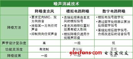
In these applications, to reduce or filter out environmental noise and improve the voice communication effect, different methods can be used, such as special noise reduction microphone, analog circuit noise reduction or digital circuit noise reduction (see Table 1). Each of these methods has its own characteristics. In comparison, the method of digital circuit noise reduction is flexible, the acoustic design complexity is low, and the noise reduction effect is superior. Of course, in addition to providing good noise reduction, portable device designers face a variety of design constraints and challenges such as size, power consumption, physical acoustic design, audio fidelity and cost.
Table 1: Comparison of different noise reduction techniques.
Advanced dual microphone real-time adaptive noise reduction technology
ON Semiconductor recently introduced the BelaSigna R261 high-performance speech capture system-on-chip (SoC) based on digital circuit noise reduction technology. The device uses advanced dual-microphone noise reduction technology to help the design provide excellent noise reduction (see Figure 1). This advanced signal processing technology accepts signals from two microphones, distinguishes between different types of signals, extracts valid speech information and suppresses environmental noise, thereby improving speech recognition.
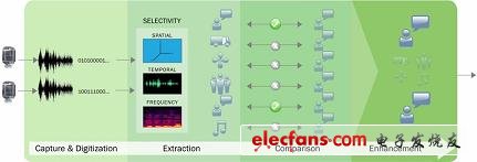
Figure 1: BelaSigna R261 uses an advanced real-time adaptive noise reduction algorithm.
The BelaSigna R261 has a built-in speech extraction algorithm in its integrated ROM memory. This algorithm utilizes one or more sensors to extract waveform propagation signals without prior knowledge of the source or sensor location. This scheme utilizes global optimization criteria while operating in the frequency, time, and air domains. There is no limit to the number of sound sources and the number of sensors, regardless of signal-to-noise ratio (SNR), ie, in low SNR and high SNR environments. Working equally well, it is ideal for applications such as cell phones and portable computers that need to extract useful speech signals from different noise domains.
This adaptive noise suppression algorithm provides 25 dB of noise rejection, which separates the required speech and ambient noise in real time, is suitable for a variety of voice sources and voices in a variety of locations, while ensuring natural sound quality (other solutions are processed The sound is unnatural, not full, and can work effectively with microphones of all qualities.
BelaSigna R261 key feature analysis
The BelaSigna R261 is a high-performance speech capture SoC that integrates a digital signal processor (DSP), voltage regulator, phase-locked loop (PLL), level shifter, and ROM memory. This high level of integration is comparable to other solutions. The bill of materials (BOM) can be reduced. As shown in Figure 2, the device supports dual-microphone direct input. The noise reduction algorithm is built into the integrated ROM memory. The DSP-based application controller provides high performance and ultra-low power consumption, provides dual-pass analog output, and supports digital microphones. Output. In addition, the built-in power management module supports supply voltages from 1.8 V to 3.3 V. The built-in on-chip PLL provides multiple frequency options and an I2C interface.
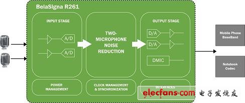 Figure 2: BelaSigna R261 high-performance voice capture SoC functional architecture diagram.
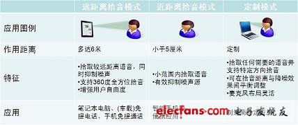
 In particular, the dual-microphone real-time adaptive noise reduction algorithm used by BelaSigna R261 provides two basic algorithm modes: long-distance pickup mode (algorithm mode 0) and close-range pickup mode (algorithm mode 1). . Optimized for long-distance pickup, Algorithm Mode 0 picks up up to 6 meters of voice while suppressing noise and supports 360-degree pickup. It is suitable for laptop, hands-free phone/meeting or mobile phone hands-free calling mode. . In this mode, even if the user is not pointing at the microphone, or even away from the microphone, it provides excellent speech intelligibility, thereby enhancing the freedom of use. Algorithm mode 1 is optimized for close-range pickup. At this time, the user is very close to the microphone (the distance is less than 5 cm), that is, picking up the voice in close range, effectively suppressing various environmental noises, and is suitable for mobile phones, learning machines, walkie-talkies, etc. Equipment that works in a noisy environment.
In addition to these two basic algorithm modes, BelaSigna R261 also provides a custom algorithm pattern to help manufacturers meet specific application needs. This algorithm mode supports special configuration and can be adjusted by loading new algorithm parameters via an external EEPROM or I2C control interface. Algorithm effects can be optimized for specific applications, microphone types, locations, and other system parameters.
Table 2: BelaSigna R261 supports different modes such as long-distance pickup, close-range pickup and customization.
As mentioned above, the BelaSigna R261 offers high integration with an adaptive noise reduction algorithm that can be directly connected to the digital microphone interface or the microphone input of the main chip (baseband processor). In addition to supporting multiple pickup modes, another important advantage of this device is that it is easy to integrate into the design, which minimizes the time and engineering required for design-in design because the design team does not have to Develop or acquire algorithms without having to design complex support and interface circuits.
The device also enables cost-conscious original equipment manufacturers (OEMs) to use inexpensive two (not necessarily matched) omnidirectional microphones in their designs, making microphone layout more flexible and eliminating the need to debug microphones on the production line, further saving Time and cost. The SoC is available in a very compact 5.3 mm2 WLCSP package (both 26-ball and 30-ball versions), which takes up much less board space than other options, even in the most space-constrained form factor of portable consumer electronics. Come on. In addition, the device consumes 15 mA at 3.3 V and consumes very little power.
BelaSigna R261 application design points
Since the BelaSigna R261 ROM-based noise reduction algorithm is very flexible, there are many possible options for the microphone layout (physical acoustic design), but the default algorithm works best only when the microphone is laid out in the following way: 1) Two microphones facing the user Mouth; 2) The intermediate point of the two microphones is located within 10 to 25 mm of each microphone. Of course, other microphone layout configurations can be used when using the custom mode.
In terms of circuit design, the BelaSigna R261 is designed to support both digital and analog processing in a single system. Due to the nature of this mixed-signal circuit, careful design of Printed Circuit Board (PCB) wiring is critical to maintaining high audio fidelity. In order to avoid coupling noise from entering the audio signal path, the digital signal is traced away from the analog signal trace. In order to avoid electrical feedback coupling, it is also necessary to isolate the input traces from the output traces.
In terms of grounding design, the ground plane should be divided into two parts, the analog ground plane (VSSA) and the digital ground plane (VSSD). These two ground planes should be connected together by a single point (ie star connection point). The star connection point should be at the ground of the capacitor at the output of the power regulator. Of course, these are just some of the issues that designers need to be aware of when applying the BelaSigna R261 design. See Reference 2 for detailed design points.
to sum up:
Portable device audio system designers need high-performance voice capture solutions that are easy to integrate into their systems while meeting their size, power, and cost requirements. As the premier high-performance silicon solution provider for energy-efficient electronics, ON Semiconductor offers the ElaSigna R261 High-Performance Speech Capture SoC a simple choice for designers. The device is highly integrated, with advanced adaptive noise reduction algorithms and supports multiple voice pickup modes, enabling smart phones, walkie-talkies, notebooks and tablets to provide clear and comfortable voice communication with high design flexibility. At the same time, the small size and low power consumption make it easy to select a low-cost microphone, so that all kinds of portable consumer electronics manufacturers can greatly improve the voice recognition and customer satisfaction, and speed up the product launch process.
What PCB designer Must Know About Impedance Control PCB
Controlled Impedance PCB Meaning
Impedance control has been one of the essential concerns and tough problems in high-speed PCB design. Impedance is the sum of the resistance and reactance of an electrical circuit. The resistance being the opposition to current flow present in all materials. In high frequency applications, controlled impedance helps us ensure that signals are not degraded as they route around a PCB. Resistance and reactance of an electrical circuit have a major impact on functionality, as certain processes must be completed before others to ensure proper operation.

Because of complex processors, USB devices and antennas are printed directly on the circuit board surface. The speed of signal switching on the circuit board increases, and the electrical characteristics of the tracks that transmit signals between devices become more and more important. Therefore, more and more PCB designs need impedance control and testing.
Impedance control technologies are quite important in high-speed digital circuit design in which effective methods must be adopted to ensure the excellent performance of high-speed PCB. The impedance of a PCB is largely determined by some factors, such as trace width, copper thickness, dielectric thickness, dielectric constant. Impedance, generally measured in Ohms. We must control the resistance and reactance of an electrical circuit to ensure the quality of signal in the complex design. For example single-ended impedance 50 ohm ±10%, differential impedance 100ohm ±10%.
When to Use Controlled Impedance
When a signal must have a particular impedance in order to function properly, controlled impedance should be used. In high frequency applications matching the impedance of PCB traces is important in maintaining data integrity and signal clarity. If the impedance of the PCB trace connecting two components does not match the components` characteristic impedance, there may be increased switching times within the device or the circuit. There may also be random errors.
Please note that we also need special instructions here:In DC circuits there is no reactance and the resistance of copper conductors is typically insignificant. However in high speed AC circuits (those with sharp changes in voltage and/or current) the reactance and thus the impedance can become very significant. This can become critical to a design's functionality because of the effects that changes in the impedance along the signals path from transmitter to receiver will have on the efficiency of power transfer as well as signal integrity. While a circuit`s speed is often expressed as the frequency of the wave form: the critical concern is the speed at which the voltage and/or current is required to change.
What Determines Controlled Impedance?
The characteristic impedance of a PCB trace is typically determined by its inductive and capacitive reactance, resistance, and conductance. These factors are a function of the physical dimensions of the trace, the dielectric constant of the PCB substrate material, and dielectric thickness. Typically PCB trace impedance can range from 25 to 125 ohms. The impedance value generated from the PCB structure will be determined by the following factors:
– Width and thickness of the copper signal trace (top and bottom)
– Thickness of the core or prepreg material on either side of the copper trace
– Dielectric constant of the core and prepreg material
– Distance from other copper features
Impedance Control In PCB Design

Electrical Impedance: A measure of opposition to time-varying electric current in an electric circuit.
The Problem: "A", "B" and "C" signals all reach the component at the same time.
The Solution: Apply Impedance to Circuit "C" to slow the signal enough for the component to first calculate ("A"+B").
Similar with a cable, the signal encounters a change of impedance arising from a change in material or geometry. Part of the signal will be reflected and part transmitted. These reflections are likely to cause aberrations on the signal which may degrade circuit performance (e.g. low gain, noise and random errors). In practice, board designers will specify impedance values and tolerances for board traces and rely on the PCB manufacturer to conform to the specification.
When rise times continue to reduce, inevitability the number of traces requiring impedance control will continue to increase. Where impedance control is needed it is important to control it accurately, calculating it with the most representative cross-section we can create.
Applications of Controlled Impedance
Controlled Impedance should be considered for PCBs used in fast digital applications such as:
– Telecommunications
– Computing 100MHz and above
– High Quality Analog Video
– Signal Processing
– RF Communication
Impedance Control PCB Manufacturing
In order to meet the growing demand of impedance control PCB, PCB manufacturers have invested a lot of money and manpower and material resources in production technology, in order to meet the production requirements of customers.
Due to the difficulty of impedance control PCB production, PCB manufacturers generally require PCB designers or purchasers to provide more detailed information and requirements, such as the type of material required, copper weight and thickness of the board, the number of layers, gerber file, so that the manufacturer can prepare the bill of materials (BOM). Impedance information should be clearly marked in Gerber file. If the necessary information is lacking, even a little key information will make it difficult or impossible for the manufacturer's engineers to know exactly what the customer needs.
Impedance-controlled PCBs are also divided into three different situations:
No Impedance Control: This is a situation where you do not need any extra design elements to ensure correct impedance because you have very loose impedance tolerance. Naturally, this will result in a faster-completed, less expensive board because the manufacturer does not have to include any special measures.
Impedance Watching: What is impedance watching? This is a situation where the designer will outline the impedance control trace and the PCB provider adjusts the trace width and dielectric height accordingly. Once the manufacturer approves these specifications, they can begin to manufacture the board. You can request a Time Domain Reflectometry (TDR) test to confirm the impedance for a fee.
Impedance Control: Actual impedance control is something you will typically only request when your design has tight impedance tolerances that could be tough to hit the first time around. When the capability limits of the manufacturer get close to the dimension requirements, it can be tough to ensure target impedance on the initial attempt.
In the case of impedance control, the manufacturer makes the circuit board achieve the target impedance as far as possible. Then they tested TDR to see if they succeeded. If not, they adjust accordingly and try again until they reach the required impedance.
Impedance Control PCB Fabricator
Impedance Control PCB is too complicated? No worry! JHY PCB engineers can help you at any time as we have three shifts. Free stack-up and impedance calculations can be offered upon request. We will work with your engineering team at the conceptual level of the PCB design to assist you to get better results in controlling impedance by choosing the suitable laminate and layer stack up.
Why Impedance Control PCB can be shipped timely all the time? As common materials are stored well in JHY PCB warehouse regularly. We have heavy copper thickness, 2oz, 3oz or more. Odd copper thickness H/1 oz, H/2 oz, 1/2 oz. Foil: 1/4 oz, H oz, 1 oz, 2 oz, 3 oz.
If you need order Impedance Control PCB, just make notes in Readme file, and send it together with Gerber, our engineer will take care of it. Have a try!
Impedance Control PCB
Blank PCB Board,Impedance Control PCB,circuit board prices,PCB With Impedance Control
JingHongYi PCB (HK) Co., Limited , http://www.pcbjhy.com