What are the benefits of using a multi-feedback (MFB) low-pass active filter tool from a vendor? Let's delve into it to get the answer.
In this exploration of the accuracy of online design tools, the RC values ​​given by the four vendor tools on the market for relatively simple second-order low-pass filters are implemented in MFB topology. This article will use these values ​​for simulation to compare the resulting filter shape to the ideal target to derive the fit error for each scenario. The nominal fit error is caused by the standard value constraint of the RC and the gain-bandwidth product (GBW or GBP) of the finite amplifier. The output point and integral noise results for each RC scheme using the same op amp model are slightly different due to differences in resistance and noise gain peaks.
The noise gain shape within the MFB filter is produced by the desired filter shape and noise gain zero. The peak noise gain of different schemes varies greatly due to the different noise gain zeros given by a particular RC scheme. The design example will illustrate these differences and also show the difference in minimum in-band loop gain (LG) for RC schemes derived from different tools.
Fitting error between nominal gain response and ideal responseThere are many ways to estimate the fit error. All of these tools have very similar response shapes over most of the frequency range, with most of the deviation occurring near the peak of the response. A simple measure of fit is to compare the f0 and Q derived from each implementation circuit with their ideal targets to derive their percentage error. Then find the root mean square (RMS) of these two errors to get a combined error indicator.
Regardless of the op amp chosen for the design, the ADI tool allows you to download simulation data - here is the LTC6240. To continue comparing the noise and loop gain of the different schemes, the RC scheme was ported to TINA while the LMP7711 was used as the public op amp for the noise simulation of each scheme. Since the ADI tool is also used for a slightly different filter shape (1.04dB peak vs 1.0dB in other tools), for comparison, the response fitting results are first isolated.
ADI target response shape:

Using the circuit in Figure 1 (and the RC number shown), the two ADI solutions will be simulated using the LTC6240 in the ADI tool and the LMP7711 in TINA (Figure 1 is the TINA setting using the LMP7711). The key requirement for an effective fit comparison is the true single pole open loop gain bandwidth product of the op amp. Testing the LMP7711 Aol (open loop gain) response using the TINA model showed a 26 MHz GBW result, which was reported as 17 MHz GBW. Prior to the simulation, the model was modified to 17 MHz (C2 was increased from 20 pF to 33.3 pF in the macro) so that the results obtained were compared to the LTC6240 simulation data from the ADI tool. To facilitate Aol testing, the LTC6240 does not appear in the TINA library, but we assume it meets the GBW = 18MHz in the data sheet.
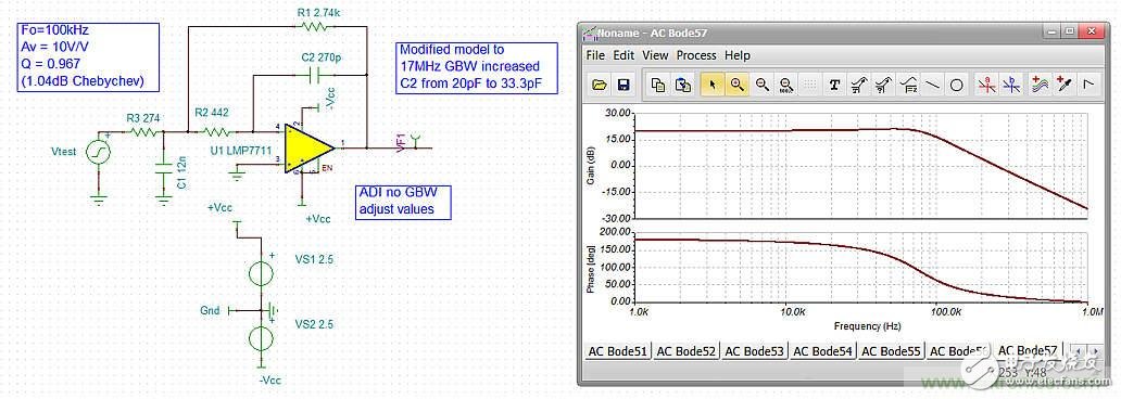
Figure 1: The ADI value of the ADI unadjusted GBW is given in TINA and the active filter emulation of the LMP7711 is used.
The first level that does not match the target is the standard resistance value selection. There are five RC values ​​to choose from, but there are only three design goals. Usually, the E24 (5% step) capacitance value is selected first, and then the final result of the E96 (1% step size) precision resistance is obtained for the three design targets. These values ​​can be placed in an ideal (infinite GBW) formula to first assess how much error is expected in this step. First select the standard capacitor value, the standard value of the three resistors will be higher and lower than the exact result. Although it is unlikely to be implemented in these current tools, in the future, a fitting proximity test can be performed on 8 standard value arrays above or below the exact value, and then the exact value is "turned" to the standard value with the least error. More often, the three exact value resistors are each selected to the nearest standard value. The fitting error is somewhat random based on the extent to which the exact value is initially close to the standard E96 resistance value.
These values ​​can then be applied to a finite GBW op amp model and simulated prior to applying the RC tolerance to arrive at a final nominal fit error. Table 1 summarizes the data downloaded from the ADI tool using the LTC6240 model and the data downloaded from TINA using the improved GBW LMP7711 model. Note that with these nominal standard RC values, no limited GBW op amp simulation can achieve the desired 100kHzf-3dB frequency within 1%.
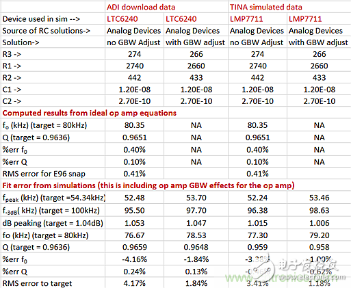
Table 1: Summary of fitting error results for ADI targets and scenarios.
The ideal op amp value assumes an infinite GBW with errors that are only caused by the selected standard resistance value. The RC value adjusted by GBW cannot be applied to the ideal formula because its target seems to be wrong. Using the actual op amp model to display the nominal results, the RC value was not adjusted for GBW, resulting in a large root mean square error of 3.4% to 4.2%. This is because this design chose an ultra-low GBW device. The ADI GBW adjusted RC value greatly improves this situation, making the nominal rms error of fo and Q only 1.2% to 1.8%. As expected, they have a slight increase in error of 0.41% over the E96 standard resistance value. Figure 2 compares these simulation results with the ideal values ​​and scales up near the peak.
These nominal response shapes are close to but not exactly the same as the target. The effect of the tolerance of the RC device further magnifies the expected response shape that has shifted the nominal result. The RC value of the gray LMP7711 is adjusted by GBW. It seems to have the worst fit in the figure and the worst fit to Q, but its RMS fit error is the smallest and fits f and f-3dB. the best. Obviously, if the nominal response has been offset relative to the target, there is still a long way to go to improve this fit to provide more target-centric extensions when including RC tolerances (note: ADI Tools Response extended envelope data downloads are also provided - but this is beyond the scope of this article.
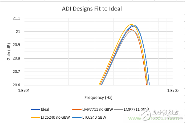
Figure 2: A magnified close-up of the response matching around the 1.04 dB target peak at 54.34 kHz.
Continue to use the RC results for TI and Intersil tools, which list slightly different goals:

These tools seem to only provide RC solutions for "ideal" op amps. In order to test the impact of using a relatively slow (17MHz, LMP7711) device, only the RC values ​​of Webench and Intersil are used here, and the results of the simulation with the 150MHz GBW OPA300 model are also displayed.
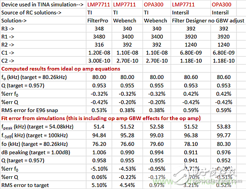
Table 2: Summary of design and target fitting errors for TI and Intersil scenarios.
For an ideal op amp formula, the initial error of the relative standard resistance seems to be in the range of 0.38% to 0.59%. Assuming an ideal op amp, downloading the first column and the second column of response data from Filterpro shows a similar initial error. When simulated using the 17MHz GBW (LMP7711) model, the error increased from 3.21% to 5.1%. Re-run with more "ideal" devices (such as the 150MHz GBW OPA300) with errors down to 1% RMS. Figure 3 shows the response shape of the design of Table 2 near the gain peak.
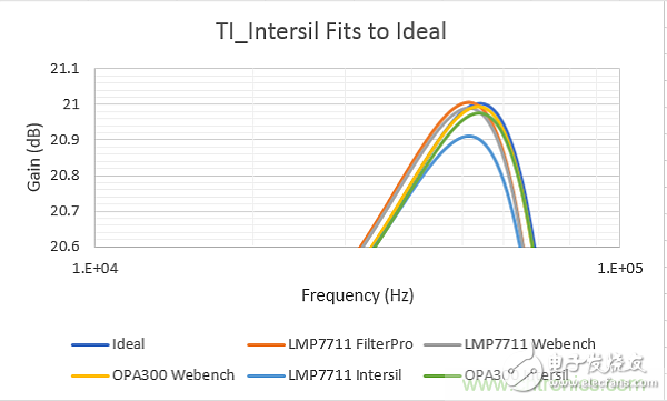
Figure 3: Close-up of the response matching amplification near the 1.0 dB target peak at 54.08 kHz.
The best fit here is the RC value from Intersil (assumed to be an ideal op amp) and the much faster OPA300. It appears that using the device at the low end of the GBW recommended by the ADI tool results in a relatively large nominal fit error. Where lower GBW (and power) devices are required, it is prudent to use an RC program that has been tuned to GBW. Obviously, using a much faster device like the OPA300 can improve the accuracy of the fit - but in these examples, the price is that the OPA300 has a current of up to 12mA, while the LMP7711 is only 1.15mA.
Output point noise and SNR for different scenariosAssuming the input voltage noise inherent in the LMP7711, LTC6240, and ISL28110 op amps is approximately 6nV to 7nV, the RC scheme of the filter is adjusted. For the sake of simplicity, the noise comparison will be done in TINA using the LMP7711 model. Check the model and the input noise in the flat band is 4.9nV/√Hz, instead of 5.9nV at the higher frequency than the 1/f turn given in the data sheet. In order to increase the apparent input voltage noise of these simulations to approximately 6.0nV as assumed in the RC scheme, it is only necessary to add a 602Ω resistor ground to the non-inverting input before performing the MFB noise comparison simulation, and then use the op amp model noise. Root mean square processing. Since this is a CMOS input amplifier, you can safely ignore the effects of input current noise. Figure 4 shows the circuit and output point noise for a GBW-adjusted RC value generated using the ADI tool. A new component in the simulation is a grounded 602Ω resistor added to the non-inverting input to generate op amp model data when combined with the inherent 4.9nV/√Hz derived from a simple 100V/V test simulation gain. The 5.9nV/√Hz data specified in the manual.
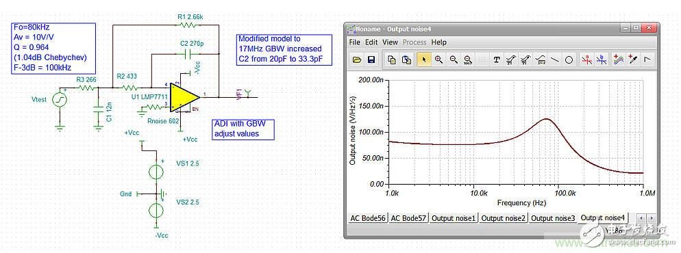
Figure 4: Example of output point noise for an RC scheme adjusted by the ADI tool using the LMP7711 model.
The point noise curve of Figure 4 shows a 1/f corner at the 1 kHz starting point, then tends to be flat in the intermediate frequency region and peaks around the resonant frequency. Due to the inherent noise gain peak (NG) of this topology, most active filter designs exhibit such noise spikes. Four design examples will use this simulation to produce flat and peak noise.
One way to look at the integrated noise is to make the SNR a specific expected maximum Vpp output. These design examples are also simulated for SNR and integrated to 1 MHz using the 4Vpp maximum output assumption (input in the TINA's noise panel with a 4Vpp RMS value of 1.414Vrms). Table 3 summarizes the noise simulation results using four designs.
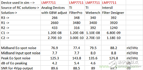
Table 3: Noise simulation results.
Figure 5 is a plot of output point noise vs. frequency for a simulation of four sets of RC values ​​in Table 3 using the LMP7711 TINA model.
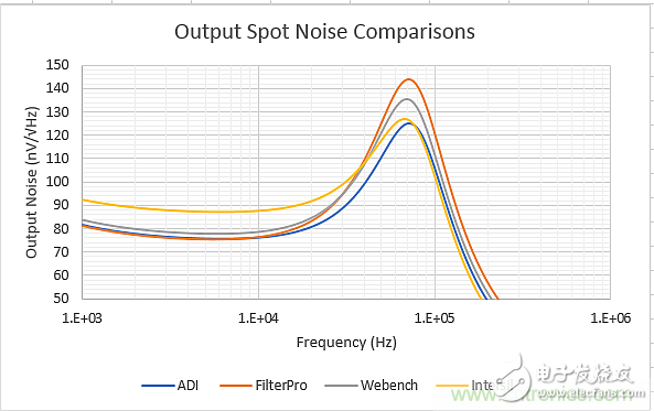
Figure 5: Simulation of output point noise simulation.
Looking at the noise map of Figure 5, the following conclusions are obtained:
The Intersil value gives the highest flatband noise (highest resistance), but the peak is lowest at this level;
The flat-band noise of the other three designs is almost the same, with the ADI design having the smallest peak;
The FilterPro design has the highest peak value because the input resistance is greater than the internal resistance of the loop;
The input reference noise in the flat band is not much larger than the 5.9 nV/Hz of the LMP7711 model + 602 Ω noise. This indicates that the resistance has been adjusted to only slightly affect the range of overall results. The difference in the R2/R3 ratio (and the resulting noise gain zero position) has a greater impact on the integrated noise and the corresponding SNR;
The signal-to-noise ratio of ADI and Intersil's RC solution is better than the FilterPro design by more than 1dB. This is because the noise gain zero of the FilterPro design is wider than the other three solutions. These differences are due to the fact that the RC schemes all target the same filter response shape.
Noise gain (NG) peak and loop gain (LG) analysis
The noise gain frequency response inherent in the MFB topology peaks with frequency. The peak is generated due to the desired frequency response pole and noise gain zero - they are controlled to produce more or less in-band peaks while still providing the desired closed loop response shape. The MFB noise gain of the circuit of Figure 1 is given by Equation 1. The numerator of the formula (used to solve the transfer function zero) is written as much as possible based on the target response shape.
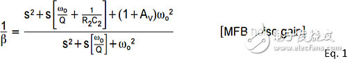
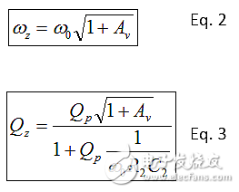
In addition to the 1/(R2C2) integration in the inner loop, the molecules are completely limited by the desired filter poles. This means that the integral link ratio can be used to move the zero point within a certain limit. The zero point of the MFB noise gain is always a real number, but can be described by the familiar ωz and Qz formats similar to the denominator in Equation 1. Qz is always "0.5, indicating that there are 2 real zeros. To obtain ωz and Qz and the zero point, the numerator portion of Equation 1 is solved, and Equations 2 and 3 are obtained, which are written according to the desired active filter poles ω0 and Qp.
The zero point falls above and below the desired filter f0, and increasing Qz to 0.5 will cause the lower zero frequency to rise. This reduces the peak noise gain with frequency and increases the passband LG for any selected op amp.
For each of the schemes in Table 3, the NG shape can be analyzed using Equation 1, and Equation 3 is used to derive Qz and the lower noise gain zero is solved. Then using Equation 1 can generate different NG versus frequency curves for the different RC schemes in Table 3, as shown in Figure 6. This shows that all solutions for the same closed loop response have large differences in peak NG.
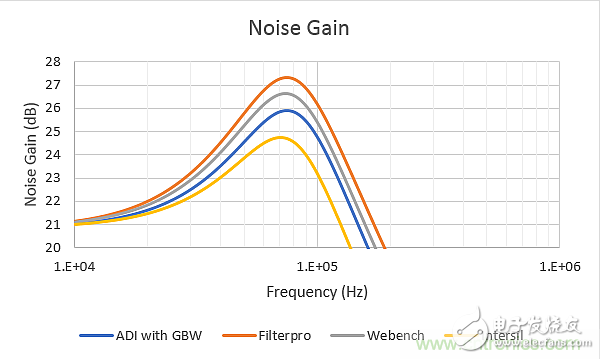
Figure 6: Noise gain response shape for different RC schemes in Table 3.
Combining the NG curve with the Aol curve of LMP7711 and generating the difference as LG gives the minimum loop gain. The example in Figure 7 calculates the noise gain of the Intersil RC scheme in Table 3, showing the 17 MHz Aol curve for the LMP7711, and the corresponding LG.
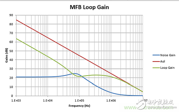
Figure 7: Noise gain and resulting loop gain for Intersil RC values ​​in Table 3 and LMP7711 Aol.
All second-order low-pass MFB LG diagrams exhibit similar features to Figure 6. Key points include:
The Aol curve of the LMP7711 uses 17MHz GBW. From the 40dB gain line, it can be seen by crossing 170kHz and multiplying by 100 times;
The NG curve shows the peak characteristics near f0. In this case, for the design example using Intersil RC values ​​in Table 3, the peak value is reduced (as shown in Figure 6);
For the desired filter shape, when NG falls above f-3dB, the LG reaches a minimum near the maximum noise gain and remains relatively flat from here to about 10 times the f-3dB frequency;
NG is close to 0dB (1V/V) at higher frequencies due to the feedback capacitance in the design. This indicates the need for a unity-gain stable op amp. The solution to this constraint is to use an additional grounding capacitor at the inverting input. In FDA-based MFB filter designs, to improve loop phase margin, a differential capacitor can be placed across the input to create a higher noise gain at the LG = 0dB crossing.
The minimum LG near the f0 and the filter response shape interact with each other in several ways:
Since the loop gain is the lowest, this will be the peak gain error frequency in the response;
This will also be the maximum closed loop output impedance over the entire response range;
The minimum loop gain also means minimum harmonic distortion suppression.
Gain bandwidth adjustment routines typically include op amp Aol effects, but rarely include output impedance peaks. LG reduces the open-loop output impedance of a particular device, but the open-loop output impedance may be very reactive, and has only recently been well modeled in modern rail-to-rail output devices.
Table 4 summarizes the noise gain Qz, the resulting lower noise gain zero, the NG peak, and the minimum loop gain for the four scheme examples given by the four different tools. The reported peak noise gain is an increase in the DC value of 20 * log (11V/V) = 20.8dB. The 11V/V DC noise gain is assumed to be driven by a zero ohm supply.
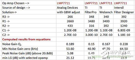
Table 4: Summary of NG Qz and lower NG zero frequencies with NG peak and LG minimum.
When possible, it is best to raise the lower noise gain zero within other constraints to bring it as close as possible to f0. The IntersilRC solution has already done this, with peaks from DC noise gain (20.8dB, 11V/V) reduced – about 2.6dB lower than the Filterpro solution. Note that the peak NG in all four solutions is significantly higher than the 1 dB target peak in the response shape. The lower noise gain zero controls the maximum NG peak, which has the greatest impact on the minimum loop gain value and SNR in the low pass active filter design where the peak is not too large. The minimum loop gain for all four designs is relatively low, which is due to the selected 17MHz GBW device. There are several reasons to use a higher GBW device (higher than the 17MHz selected here):
The nominal deviation of the response shape is lower than the desired target;
The minimum LG of the f0 area is higher;
Lower output harmonic distortion;
Lower closed-loop output impedance – interacts with the accuracy of the response shape and the ability to accurately drive the load.
Starting with the smallest GBW design here, using a faster op amp will directly affect the minimum LG. For example, using a 150MHz OPA300 and a 17MHz LMP7711 will increase the minimum LG in Table 4 by 20log(150/17) = 18.9dB. Time domain-oriented applications generally accept lower minimum LGs. Where minimum harmonic distortion is required, consider a device that is faster and has the least increase in quiescent current.
Table 5 summarizes the performance of the four design examples using the modified LMP7711 model. Obviously, small differences in the RC scheme can result in significantly different final nominal performance.
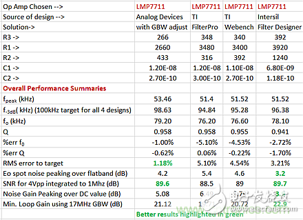
Table 5: Summary of LMP7711 op amp selection results.
Summary of comments and suggestionsThis paper evaluates the nominal fit accuracy and some dynamic ranges in detail. All four tools used an ideal op amp and achieved good nominal fitting accuracy—the nominal fit error was 0.6% when the E96 step resistance value was chosen. All response shapes deviate from the target, including a true op amp – so you should not expect a perfect nominal fit that fits your goal. Operation with a minimum gain-bandwidth amplifier can significantly reduce power consumption, but should be used in conjunction with the GBW adjustment method to reduce the nominal fit error.
Newer tools (ADI, Webench, and Intersil) can adjust the R value to fit the range of the op amp's inherent input noise specifications. However, the main mechanism for distinguishing the integral noise is the layout of the noise gain zero. The Intersil tool increases Qz and reduces noise gain peaks. It is unclear how the other three tools treat this strategy.
Tool development and design recommendations:
Considering the metrics mentioned in this article, pay attention to balancing GBW margin and power consumption when selecting an amplifier;
Verify the op amp model as much as possible before testing and make changes as needed to improve the effectiveness of the results;
Utilize the GBW adjustment algorithm to extend the applicable space of the solution to much lower speed/power op amps and/or improve nominal fit accuracy;
Placing the RC solution towards a higher noise gain Qz, which will increase the SNR and improve the LG in the NG peak region;
For each second class, it is allowed to set the target pole directly. In this way, designs generated with some of the more powerful third-party tools can be implemented in the op amp vendor tool to better bind the RC solution to the op amp parameters;
Leave a 2% capacitance tolerance in the 5% E24 step and a 0.5% resistor tolerance in the 1% E96 step. They are easier to obtain than full E48 capacitor series or E192 resistor step values;
The MFB scheme is extended to include the attenuation phase. Unlike the SKF topology, the inverting MFB design is ideal for attenuators - there are no constraints in the implementation or formula, and users are free to choose a VFA op amp or a precision fully differential amplifier (FDA), which is very useful.
The next step in active filter design is to select the RC tolerance and then run the Monte Carlo program to evaluate the response spread of the nominal starting point considered here. It should be noted that the full 2% E48 series C0G (or NPO) capacitors are not readily available, but the slightly higher price of the 2% tolerance capacitors in the 5% E24 series is sufficient. The resistance is usually chosen to be 1% E96. However, the 0.5% tolerance value in the E96 step is easier to obtain than the full E192 series. The response spreads significantly around the nominal value, from 5% capacitance and 1% resistance to 2% capacitance and 0.5% resistance, and adds only a small BOM cost (including the large op amp cost).
Off grid system mainly refers to a new energy power supply system relying on storage Battery as the backup. In the case of sunlight during the day, the solar battery supplies power to the load and stores excess power in the battery; When the sunshine is insufficient or during the night and cloudy days, battery serves as the backup to ensure all power is sent to the load till the next sunny day. Repeat continuously. Pure solar power supply has the characteristics of high reliability, low maintenance and long service life.
Solar Power System,Solar System For Home,Solar Power Generator,Solar Energy Storage System
Wuxi Sunket New Energy Technology Co.,Ltd , https://www.sunketsolar.com