Abstract: The following applicaTIon note provides an insight into the mathemaTIcal definiTIons of quanTIzation and thermal noise, parameters which can significantly affect the signal-to-noise ratio (SNR) and signal-to-noise plus distortion (SINAD) specifications of analog-to -digital converters (ADCs) in RF receiver applications. It concludes by comparing their impact on the effective noise figure for a Nyquist and oversampling ADC.
When using a Nyquist analog-to-digital converter (ADC) in a sampling or sub-sampling receiver application, an RF designer needs to know the ADC's effective noise figure, in order to perform determine the cascaded noise figure for the complete receiver line- up.
The following discussion assumes that the noise is flat across the converter's Nyquist band and provides a designer with the means to determine an estimate for the ADC effective noise figure. Additionally, this article provides a direct comparison of the effective noise figure for a Nyquist ADC and an oversampling ADC.
The signal-to-noise ratio (SNR) of an ADC is the ratio of the signal power to the non-signal power. Non-signal power includes thermal noise, quantization noise, and other residual errors in the converter, measured in the Nyquist bandwidth (fSAMPLE / 2) of the ADC. SNR is typically defined for a continuous sinewave signal applied to the ADC input at some level below the full-scale (FS) level of the converter, usually 0.5dB to 1dB. The ADC converts the signal into discrete output levels using a nonlinear process. The smallest discrete step is called the quantization level, which is a function of the ADC resolution, or number of bits. There is a difference (or error) between the actual sinewave value and the quantized level. The error can be any value within the quantization level resulting in an expression for an ideal converter
SNR = (1.763 + 6.02 × b) dB,
where b is the data converter's number of bits.
Unfortunately, numerous factors degrade the ADC's ideal performance resulting in a lower SNR value and higher effective noise figure value. These factors include thermal noise, clock jitter (especially for higher input frequencies having high slew rates), and subranging errors. Large-scale device nonlinearities also create harmonic spurs, however these harmonics are usually excluded from SNR calculations. In practice, an anti-alias filter with at least 10dB of attenuation should be placed in front of the ADC to prevent noise upstream of the converter from being aliased back into the converter's Nyquist band.
The following parameters are needed to determine the effective noise figure for the Nyquist ADC:
Full-Scale Power Level: The maximum allowable full-scale power level (in dBm) that can be applied to the ADC analog input is determined from the maximum ADC input voltage (clip point) and analog input terminating resistance. The converter's input voltage range is typically specified in Volts peak-to-peak (VP-P), from which the peak voltage (VP) can easily be found.
The corresponding RMS level is:
Vrms = VP / √2 = VP × 0.707
The signal power at the ADC input is found knowing Vrms and RIN:
Signal power = (Vrms²) / RIN (Watts)
The full-scale signal power (dBm) is calculated as:
Signal power = 10 × log (((Vrms²) / RIN) × 1000mW / Watt) = 10 × log ((Vrms²) / RIN) + 30dB
ADC SNR: The SNR value is found either in the manufacturer's data sheet or can be determined by the users own measurements at the desired input frequency. The data sheet will provide the conditions from which the SNR value was determined. If the user measures the SNR directly in the intended application, all circuit noise contributions will be taken into account in the measured data, which provides the user with the most accurate SNR estimate. (Note: Remember not to include spurs in an SNR measurement. For a noise figure calculation, only SNR, not SINAD, is of interest). Both the SNR value in the data sheet and the measured value take into account the total integrated noise in the Nyquist band. The converter's noise power is normalized to a 1Hz bandwidth by simply subtracting 10 × log (fSAMPLE / 2) from the SNR value. (This provides a dBc / Hz unit and must be normalized to the full-scale level of the converter to achieve dBm / Hz). This places the SNR noise level (in dBm) in a 1Hz bandwidt h, which can be directly compared to the input noise of the converter, which is the theoretical thermal noise floor limit, KTB.
KTB is calculated as follows:
KTB = 4.002 × 10⁻²¹ Watts (or in log form = -174dBm), where
K = Boltzmann's constant = 1.381 × 10⁻²³W / Hz / K,
T = 290 K at room temperature
B = Normalized bandwidth of 1Hz
To determine the effective ADC noise figure, refer to Figure 1 and follow the steps below:
Determine the converter's full-scale level (in dBm) knowing the maximum allowable VP-P and input terminating resistance, RIN. Note the level from which SNR is either specified in the manufacturer's data sheet or measured by the user (usually 0.5dB to 1dB below full-scale). Knowing the SNR value, calculate the converter's integrated Nyquist band noise power. Knowing the sample rate, calculate 10 × log (fSAMPLE / 2). Determine the converter's noise power in a 1Hz bandwidth by subtracting (4) from (3). Calculate KTB for B = 1Hz (equal to -174dBm at room temperature). Subtract KTB from the normalized Nyquist band noise power to determine the ADC effective noise figure.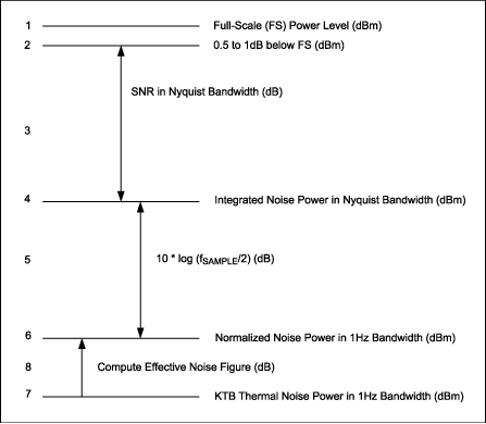
Figure 1. Steps to determine effective ADC noise figure.
Observations As the sample rate is doubled, the effective noise figure decreases by 3dB because the same input noise power is spread over twice the bandwidth thereby increasing SNR. The most accurate estimate of SNR is obtained using measured data since the user's clock jitter and other noise sources are represented in the measurement. Device nonlinearities usually don't affect an SNR measurement since harmonics are excluded from the SNR characterization of a device. If a user makes an SNR measurement, care must be taken that the test setup does not add 'false 'noise, which will not be present in the actual circuit. As RIN is lowered, the full-scale power level increases, thereby increasing the effective noise figure for a constant SNR. Figure 2 shows a direct comparison of the effective noise figure for a Nyquist ADC and an oversampled ADC. The noise density for the oversampled converter is defined in the frequency bandwidth for which the converter is designed, and the SNR is normaliz ed to that particular bandwidth to obtain the spot noise in dBc / Hz.
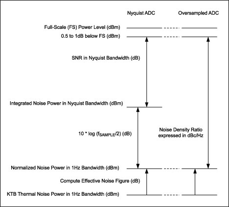
Figure 2. Compare effective noise figure for Nyquist ADC and oversampling ADC. Example Assume the full-scale input level for both converters is 2Vp-p and the device input terminating resistance is 200Ω. The full-scale power level is: Signal Power = 10 × log ((Vrms²) / RIN) + 30dB = + 4dBm. Assume the measured SNR value for a 12-bit converter sampled at 65Msps at the user's desired input frequency is 69dB (for a -1dBFS input level). The converter's integrated noise power in the Nyquist band is calculated as: + 4dBm-1dB-69dB = -66dBm. Calculate 10 × log (fSAMPLE / 2) = 10 × log (65Msps / 2) = 75.1dB. The converter's normalized Nyquist band noise power is found by subtracting 75.1dB from -66dBm resulting in -141.1dBm in a 1Hz bandwidth. The resulting effective ADC noise figure = -141.1dBm-KTB = -141.1dBm-(-174dBm) = 32.9dB. As a comparison, the oversampled ADC noise density would be 144.1dBc / Hz or 145.1dBFS / Hz in order to obtain the same effective noise figure. ConclusionAn RF de signer can trade off several parameters to optimize the ADC effective noise figure when using the device in a sampling, sub-sampling, or oversampling receiver architecture. These parameters include ADC clock rate, terminating resistance, clock jitter, and nyquist band filtering, as discussed in this article.
References Digital Techniques for Wideband Receivers, James Tsui, Artech House Publishers, 1995.
Software Ratio Architecture, Joseph Mitola III, John Wiley & Sons, Inc., 2000.
When using a Nyquist analog-to-digital converter (ADC) in a sampling or sub-sampling receiver application, an RF designer needs to know the ADC's effective noise figure, in order to perform determine the cascaded noise figure for the complete receiver line- up.
The following discussion assumes that the noise is flat across the converter's Nyquist band and provides a designer with the means to determine an estimate for the ADC effective noise figure. Additionally, this article provides a direct comparison of the effective noise figure for a Nyquist ADC and an oversampling ADC.
The signal-to-noise ratio (SNR) of an ADC is the ratio of the signal power to the non-signal power. Non-signal power includes thermal noise, quantization noise, and other residual errors in the converter, measured in the Nyquist bandwidth (fSAMPLE / 2) of the ADC. SNR is typically defined for a continuous sinewave signal applied to the ADC input at some level below the full-scale (FS) level of the converter, usually 0.5dB to 1dB. The ADC converts the signal into discrete output levels using a nonlinear process. The smallest discrete step is called the quantization level, which is a function of the ADC resolution, or number of bits. There is a difference (or error) between the actual sinewave value and the quantized level. The error can be any value within the quantization level resulting in an expression for an ideal converter
SNR = (1.763 + 6.02 × b) dB,
where b is the data converter's number of bits.
Unfortunately, numerous factors degrade the ADC's ideal performance resulting in a lower SNR value and higher effective noise figure value. These factors include thermal noise, clock jitter (especially for higher input frequencies having high slew rates), and subranging errors. Large-scale device nonlinearities also create harmonic spurs, however these harmonics are usually excluded from SNR calculations. In practice, an anti-alias filter with at least 10dB of attenuation should be placed in front of the ADC to prevent noise upstream of the converter from being aliased back into the converter's Nyquist band.
The following parameters are needed to determine the effective noise figure for the Nyquist ADC:
Full-Scale Power Level: The maximum allowable full-scale power level (in dBm) that can be applied to the ADC analog input is determined from the maximum ADC input voltage (clip point) and analog input terminating resistance. The converter's input voltage range is typically specified in Volts peak-to-peak (VP-P), from which the peak voltage (VP) can easily be found.
The corresponding RMS level is:
Vrms = VP / √2 = VP × 0.707
The signal power at the ADC input is found knowing Vrms and RIN:
Signal power = (Vrms²) / RIN (Watts)
The full-scale signal power (dBm) is calculated as:
Signal power = 10 × log (((Vrms²) / RIN) × 1000mW / Watt) = 10 × log ((Vrms²) / RIN) + 30dB
ADC SNR: The SNR value is found either in the manufacturer's data sheet or can be determined by the users own measurements at the desired input frequency. The data sheet will provide the conditions from which the SNR value was determined. If the user measures the SNR directly in the intended application, all circuit noise contributions will be taken into account in the measured data, which provides the user with the most accurate SNR estimate. (Note: Remember not to include spurs in an SNR measurement. For a noise figure calculation, only SNR, not SINAD, is of interest). Both the SNR value in the data sheet and the measured value take into account the total integrated noise in the Nyquist band. The converter's noise power is normalized to a 1Hz bandwidth by simply subtracting 10 × log (fSAMPLE / 2) from the SNR value. (This provides a dBc / Hz unit and must be normalized to the full-scale level of the converter to achieve dBm / Hz). This places the SNR noise level (in dBm) in a 1Hz bandwidt h, which can be directly compared to the input noise of the converter, which is the theoretical thermal noise floor limit, KTB.
KTB is calculated as follows:
KTB = 4.002 × 10⁻²¹ Watts (or in log form = -174dBm), where
K = Boltzmann's constant = 1.381 × 10⁻²³W / Hz / K,
T = 290 K at room temperature
B = Normalized bandwidth of 1Hz
To determine the effective ADC noise figure, refer to Figure 1 and follow the steps below:
Determine the converter's full-scale level (in dBm) knowing the maximum allowable VP-P and input terminating resistance, RIN. Note the level from which SNR is either specified in the manufacturer's data sheet or measured by the user (usually 0.5dB to 1dB below full-scale). Knowing the SNR value, calculate the converter's integrated Nyquist band noise power. Knowing the sample rate, calculate 10 × log (fSAMPLE / 2). Determine the converter's noise power in a 1Hz bandwidth by subtracting (4) from (3). Calculate KTB for B = 1Hz (equal to -174dBm at room temperature). Subtract KTB from the normalized Nyquist band noise power to determine the ADC effective noise figure.
Figure 1. Steps to determine effective ADC noise figure.
Observations As the sample rate is doubled, the effective noise figure decreases by 3dB because the same input noise power is spread over twice the bandwidth thereby increasing SNR. The most accurate estimate of SNR is obtained using measured data since the user's clock jitter and other noise sources are represented in the measurement. Device nonlinearities usually don't affect an SNR measurement since harmonics are excluded from the SNR characterization of a device. If a user makes an SNR measurement, care must be taken that the test setup does not add 'false 'noise, which will not be present in the actual circuit. As RIN is lowered, the full-scale power level increases, thereby increasing the effective noise figure for a constant SNR. Figure 2 shows a direct comparison of the effective noise figure for a Nyquist ADC and an oversampled ADC. The noise density for the oversampled converter is defined in the frequency bandwidth for which the converter is designed, and the SNR is normaliz ed to that particular bandwidth to obtain the spot noise in dBc / Hz.
Figure 2. Compare effective noise figure for Nyquist ADC and oversampling ADC. Example Assume the full-scale input level for both converters is 2Vp-p and the device input terminating resistance is 200Ω. The full-scale power level is: Signal Power = 10 × log ((Vrms²) / RIN) + 30dB = + 4dBm. Assume the measured SNR value for a 12-bit converter sampled at 65Msps at the user's desired input frequency is 69dB (for a -1dBFS input level). The converter's integrated noise power in the Nyquist band is calculated as: + 4dBm-1dB-69dB = -66dBm. Calculate 10 × log (fSAMPLE / 2) = 10 × log (65Msps / 2) = 75.1dB. The converter's normalized Nyquist band noise power is found by subtracting 75.1dB from -66dBm resulting in -141.1dBm in a 1Hz bandwidth. The resulting effective ADC noise figure = -141.1dBm-KTB = -141.1dBm-(-174dBm) = 32.9dB. As a comparison, the oversampled ADC noise density would be 144.1dBc / Hz or 145.1dBFS / Hz in order to obtain the same effective noise figure. ConclusionAn RF de signer can trade off several parameters to optimize the ADC effective noise figure when using the device in a sampling, sub-sampling, or oversampling receiver architecture. These parameters include ADC clock rate, terminating resistance, clock jitter, and nyquist band filtering, as discussed in this article.
References Digital Techniques for Wideband Receivers, James Tsui, Artech House Publishers, 1995.
Software Ratio Architecture, Joseph Mitola III, John Wiley & Sons, Inc., 2000.
24V Lithium Battery Charger,Lithium Polymer Battery Charger,24V Bike Lithium Battery Charger,24V Bicycle Lithium Battery Charger
Changxing Deli Technology Co., Ltd. , https://www.delipowers.com