Simulation design and research of the radio frequency front end of VHF frequency hopping radio receiver
With the rapid development of modern electronic technology and wireless communication technology, the application of radio communication is becoming more and more widespread, and household appliances are increasingly popular. As an important part of the receiver, the radio frequency front end mainly converts the received high frequency signal into an intermediate frequency signal. The RF front-end circuit plays a vital role in the performance of the entire receiving system. Its ability to detect small signals directly determines the sensitivity of the receiver; its ability to adapt to large signals determines the dynamic range of the receiver; good linearity can be reduced Intermodulation distortion and intermodulation distortion in the system. The article focuses on using the powerful ADS (Advanced Design System) simulation software developed by Agilent to simulate the RF front-end of the receiver to obtain reliable and superior performance indicators of the RF front-end, shortening production design time, reducing production costs, and improving products the quality of.
1 The specific indicators of the RF front end are based on the receiver's performance requirements such as sensitivity, noise figure, selectivity, dynamic range, mirror image suppression, and intermediate frequency suppression. The technical indicators assigned to the front end are: (1) Frequency range: 30 .000 ~ 87.975. MHz; (2) Gain: 13 ± 2 dB (high sensitivity), 0 ± 2 dB (low sensitivity); (3) Image frequency suppression: 30 ~ 58.975 MHz≥80 dB, 59 ~ 87.975 MHz≥75 dB; (4) With high and low sensitivity options.
2 RF front-end simulation model and overall design The block diagram of the RF front-end circuit in this article is shown in Figure 1.
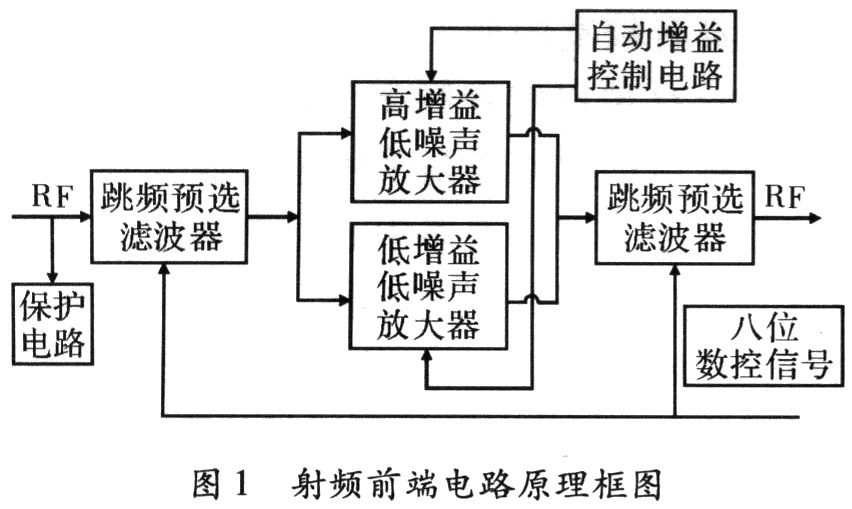
As can be seen from Figure 1, the front-end circuit consists of a protection circuit, a frequency-hopping preselection filter, a low-noise amplifier and an automatic gain control circuit. Among them, the protection circuit is the guarantee that the receiver's RF front-end can continue to work well in the modern complex electromagnetic environment to prevent the receiver from being damaged due to strong signals; the frequency hopping pre-selection filter is to select the receiver's operating frequency signal and filter it out Other clutter, improve the selectivity and suppression of the receiver; low-noise amplifier achieves undistorted amplification of the received weak signal, improve the sensitivity and dynamic range of the receiver; AGC circuit detects the signal proportional to the RF signal through the detector , And rectify it into DC voltage, compare it with the reference level through the comparator, and then input the terminal, which is controlled by the terminal, so as to realize the gain control of the LNA and improve the adaptability and stability of the receiver. This is a unique aspect of the RF front-end design.
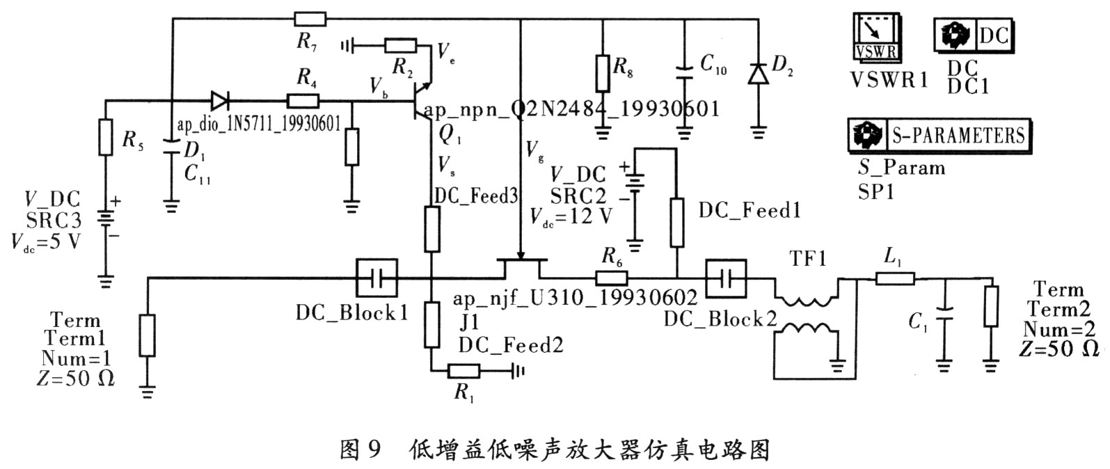
According to the principle block diagram of the front end, a simulation circuit diagram is constructed in the ADS, and the RF front-end circuit diagram under the condition of high sensitivity is shown in FIG. 2. The circuit diagram of the RF front-end under low sensitivity is shown in Figure 3.
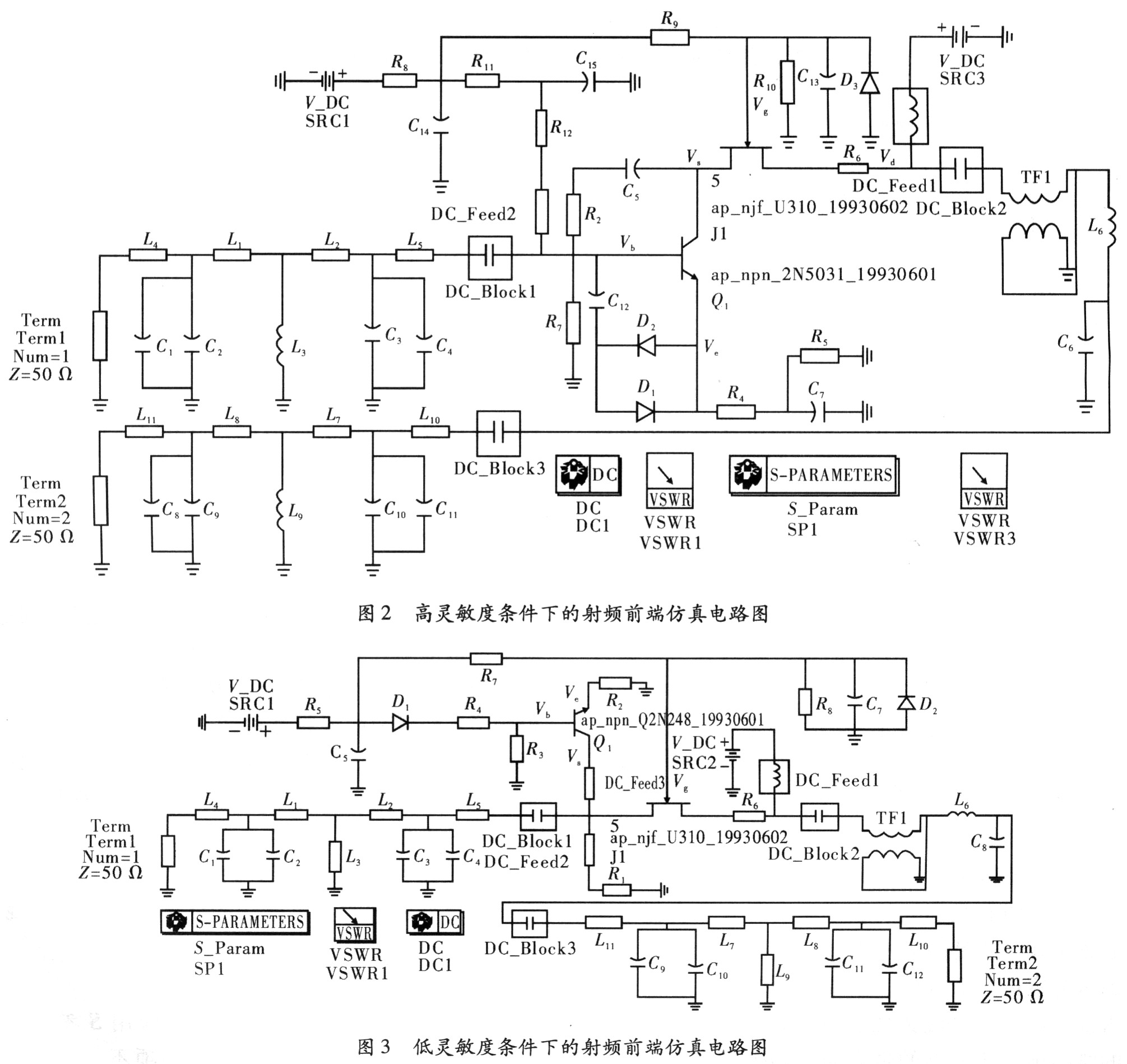
The amplifier device used in Figure 2 is the transistor 2N5031 and the field effect transistor U310; the cascade structure is used in the circuit structure to ensure sufficient power gain, and the first-stage transistor circuit uses negative feedback technology to ensure the stability of the amplifier. The amplifier device used in Fig. 3 is a field effect tube V310, which has the characteristics of high gain, low noise, and high stability.
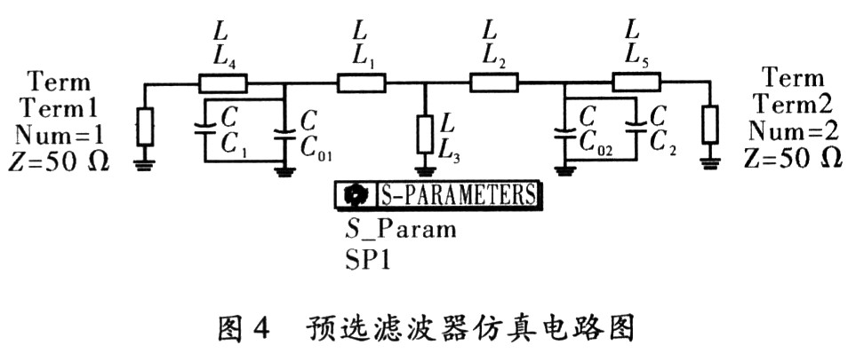
2.1 Simulation of numerical control frequency hopping preselection filter The basic function of numerical control frequency hopping preselection filter is to selectively pass the frequency, select the required signal and suppress the unnecessary signal. The main concerns of filter design are the magnitude of insertion loss, phase change, and the ability to suppress undesired signals generated by the signal through the filter. Considering that the designed receiver works in the frequency range of 30-87.975 MHz, and hopes to achieve full-band coverage and maintain a high reception sensitivity, it is best to choose to use an electric tuning filter, and the selected electric tuning The filter should have a wider tuning range, faster electrical tuning speed and higher Q value to achieve frequency preselection. The digital frequency hopping pre-selected filter designed in this project is a double-tuned filter that uses a logic chip to control the capacitor bank to achieve the center frequency tuning of the filter. In the connection diagram in ADS, as shown in Figure 4, the capacitance of the capacitors C01 and C02 is changed through the tuning control to obtain a simulation of the filter using different capacitor banks.

From the simulation results of (a), (b), (c) in Figure 5, it can be seen that the filter bandwidth is 3.9 MHz and the insertion loss is 5.352 dB when the center frequency is 86.5 MHz. When the center frequency is 60.5 MHz, the bandwidth of the filter is 2.6 MHz, and the insertion loss is 4.375 dB. When the center frequency is 30.0 MHz, the bandwidth of the filter is 1.5 MHz, and the insertion loss is 5.764 dB. Bandwidth and insertion loss appear different values ​​at each frequency point. One of the reasons is to change the center frequency by changing the capacitance value. The other reason is that during the simulation, L3 is set to a fixed value, so the frequency Overcoupling occurs at the high end, and undercoupling occurs at the low end of the frequency. In actual circuit design, L3 is the parasitic inductance of inductance L1, L2, and its value is changing. It can also be seen from the simulation results that the frequency response obtained by the filter is asymmetric, and the attenuation rate of the signal above the center frequency is greater than that below the center frequency, because the designed frequency hopping preselection filter It is caused by inductive coupling. If capacitive coupling is used, it is mirrored with the simulation result. In general, the designed frequency hopping pre-filters have both the insertion loss and bandwidth that meet the design requirements of the system. Among them, the insertion loss (4 ~ 6 dB) and bandwidth (1 ~ 4 MHz) are better implemented. In addition, the frequency selection filter function.
2.2 Simulation of Low Noise Amplifier (LNA) The Low Noise Amplifier (LNA) is an important part of the RF front-end of the receiver. The low-noise amplifier has the following characteristics: First, it is located at the forefront of the receiver, and the smaller the noise, the better. In order to suppress the influence of the noise at all levels on the system, a certain gain is required, but in order not to overload the subsequent mixer and produce nonlinear distortion, the gain cannot be too large, and the amplifier should be stable in the operating frequency band . Secondly, the signal it receives is very weak, the low noise amplifier must be a small signal linear amplifier. Moreover, due to the influence of the transmission path, the strength of the signal changes. While receiving the signal, it may be accompanied by many strong interference signals. Therefore, the amplifier needs to have a sufficient linear range.
2.2.1 LNA stability analysis
When designing small-signal high-frequency amplifiers, it is also an indispensable procedure to use S-parameters to evaluate the oscillation tendency of active components. Stability means that the active component can work stably after connecting any impedance at the input and output ends, or when it is combined with some impedance, it will cause oscillation. The former is called unconditional stability, and the latter is called latent instability. The stability of the active component can be determined by the L-shaped stability factor K of the S parameter. Before exporting K, you need to calculate

Lollet stability factor K is

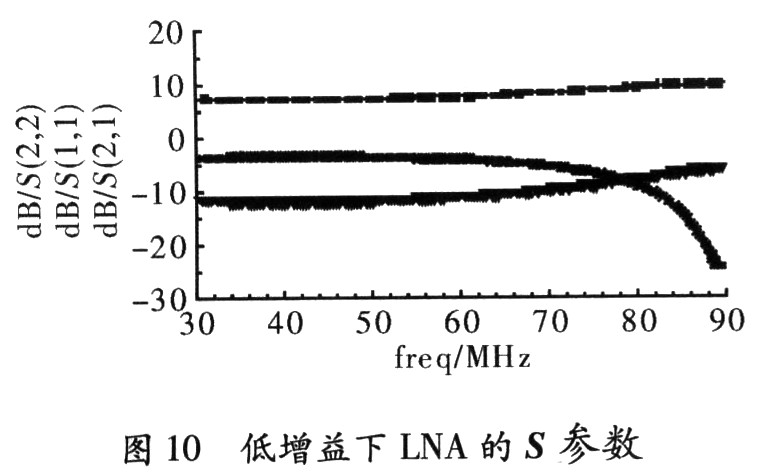
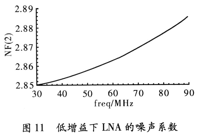
2.2.2 Simulation of high gain low noise amplifier
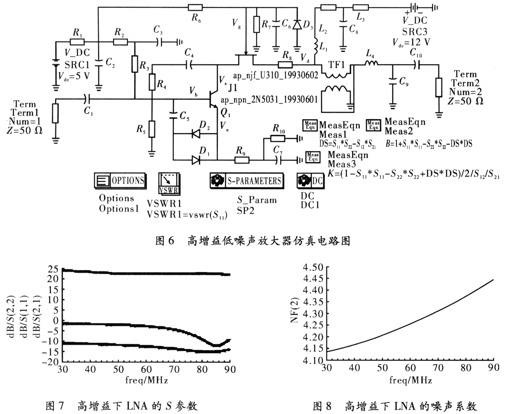
If K> 1, the active component is unconditionally stable and can be used in combination with any signal source impedance or load. Conversely, if 0 From the simulation data in Table 1, we can see that the designed RF front-end has reached the design performance index and has a certain improvement, especially in the image suppression is much better than the design requirements. 4 Conclusion From the analysis of RF front-end performance index data obtained from simulation, the gain is relatively flat in the entire working frequency band, and the suppression of the RF front-end is good, and the noise figure is low, which meets the expected design index requirements and achieves high and low Sensitivity selection, automatic gain control function. Compared with the original front-end performance, the suppression and noise figure have been greatly improved, which laid a certain foundation for the actual circuit design in the next step, shortened the product design cycle, and reduced the design cost. Kitchen Appliance,Small Kitchen Appliance Cooker,Counter Top Electric Cooker,Electric Hotplate Cooker Shaoxing Haoda Electrical Appliance Co.,Ltd , https://www.zjhaoda.com