WLAN Reference Design with the MAX2830
Abstract: This reference design is a complete RF front-end soluTIon designed to meet the WLAN IEEE® 802.11b / g standard. Using the MAX2830 RF transceiver, the design is capable of accommodaTIng full range of 802.11g OFDM data rates (6, 9 , 12, 18, 24, 36, 48, and 54Mbps) and 802.11b QPSK data rates (1, 2, 5.5, and 11Mbps). This soluTIon offers high performance, small size, and low BOM cost.
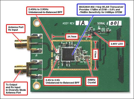
Figure 1. The WLAN reference design features the MAX2830 RF transceiver.
| Important Design Features |
High-Performance Rx NF <6dB (typ); Tx Output 15dBm (typ) Small Size: 17mm x 24.7mm Platform Design for MulTIple Form-Factors such as Card Bus and Compact Flash
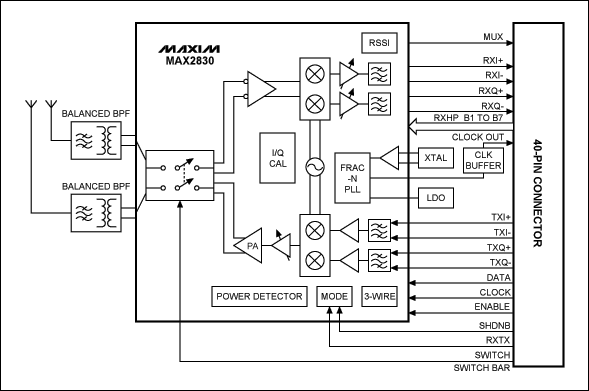
Figure 2. Block diagram of the WLAN reference design.
| Lab Measurements |
| ||||||||||||||||||||||||||||||||||||||||||||||||||||||||||||||||||||||||||||||||||||||||||||||||||||||||
| Operating Characteristics |
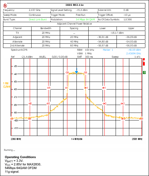
Figure 3. ACPR performance at Tx power = 15.7dBm, EVM <5.6%.
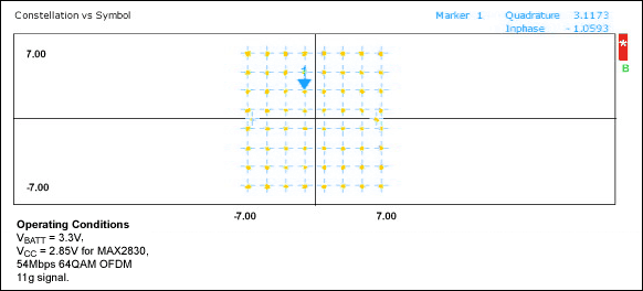
Figure 4. Rx I / Q constellation diagram at RF input = -40dBm, 54Mbps 64QAM, EVM = 2.2%.
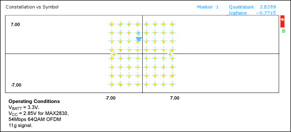
Figure 5. Rx I / Q constellation diagram at PIN = -65dBm, 54Mbps 64QAM. The EVM is only 4.2%, which is better than the 9% requirement for sensitivity.
| Detailed Description |
This reference design is suitable for the full range of 802.11g OFDM data rates (6, 9, 12, 18, 24, 36, 48, and 54Mbps) and 802.11b QPSK data rates (1, 2, 5.5, and 11Mbps) at Corresponding sensitivity levels. Using the MAX2830 chipset eliminates the need for external SAW filters, a RF switch, and a PA. Only a RF filter, RF balun, and a small number of passive components are required to form a complete 11b / g WLAN RF front-end solution that delivers high performance in a small PCB form-factor.
IEEE is a registered service mark of the Institute of Electrical and Electronics Engineers.
Rectifier bridge is to seal the rectifier tube in a shell. Points full bridge and half bridge. The full bridge connects the four diodes of the connected Bridge Rectifier circuit together. The half bridge is half of four diode bridge rectifiers, and two half bridges can be used to form a bridge rectifier circuit. One half bridge can also be used to form a full-wave rectifier circuit with a center-tapped transformer. Select a rectifier bridge to consider. Rectifier circuit and operating voltage.
Bridge Rectifier
Bridge Rectifier,Original Bridge Rectifier,Full Bridge Rectifier ,Diodes Bridge Rectifier,Single Phase Rectifier Bridge, Three Phase Bridge Rectifier
YANGZHOU POSITIONING TECH CO., LTD. , https://www.yzpst.com