OLED mainstream production technology
Evaporation technology
First of all, to understand the evaporation technology, this has to start from the structure of OLED. As shown in the figure below, the typical structure is to make a layer of tens of nanometers thick luminescent material on the ITO glass. The ITO transparent electrode and the metal electrode respectively add voltage as the anode and cathode electrodes of the device, and drive electrons and holes under a certain voltage. Injection from the cathode and the anode to the electron and hole transport layers, respectively, electrons and holes migrate to the light-emitting layer through the electron and hole transport layers, respectively, and meet in the light-emitting layer to form excitons and excite the light-emitting molecules. Visible light is emitted by radiation relaxation. Radiation light can be observed from the ITO side, and the metal electrode film also functions as a reflective layer.
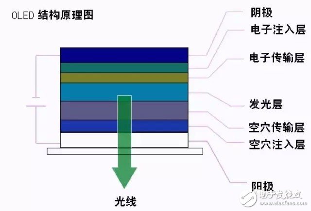
OLED structure schematic
Of course, the structure is much more complicated when it comes to the entire panel, including isolation columns, insulation layers, and the like between sub-pixels. AMOLED also has a TFT backplane that controls each pixel switch.
OLED pixel structure diagram
In simple terms, evaporation is the process of heating in a vacuum, electron beam bombardment heating and laser heating to evaporate the vaporized material into atoms or molecules, which then move in a straight line with a large free path, colliding with the surface of the substrate. Condensation to form a film.
The core equipment for the manufacture of OLED panels by evaporation technology is the vapor deposition machine. This equipment is upstream of the panel manufacturing company. The main supplier is a company named Canon Tokki under Canon. With the turmoil in the global OLED market, Tokki continues to invest in development capacity, but it is still difficult to meet customer needs. It is said that Tokki's annual steaming machine capacity is also a few units. Large customers such as LG Display have to lose their orders because of the limited number of vapor deposition machines.
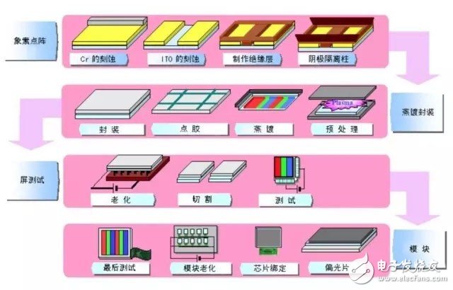
Typical process flow of PMOLED
(Note: PMOLED is also an OLED, but the structure is simpler than AMOLED, no TFT.)
Printing Technology
In addition to the steaming up of each pixel "bulb" of the OLED screen, you can also choose to "print" it out. An example is an inkjet printer that ejects ink onto a paper to present a document or picture. The printed display is a process for making a film of an organic material using a printing method. After the printing display is realized, different panels can be printed. If the "spray" is an OLED material, that is an OLED panel; the "spraying" is a quantum dot material, that is, a quantum dot display panel. Printing OLED, simply speaking, is to accurately deposit different color polymer luminescent material solutions in the isolation column groove of the ITO glass substrate through a plurality of printing nozzles on the inkjet printing device, and the solvent will volatilize to form a thickness of about 100 nm. The thin layer constitutes a pixel that can emit light.
Why is print display technology the next generation display revolution? The vacuum evaporation process, which is limited by equipment and technology, makes it difficult to fabricate large-sized fine metal masks, which makes the process unusable for the manufacture of large-sized panels. During the evaporation process, the organic material gas is deposited on the glass substrate without any difference, resulting in low material utilization. Perhaps because there is no need for vacuum evaporation of the cavity, no need for precision metal masks, no color filters, etc., at the CES show in 2013, Panasonic demonstrated a self-developed "printing" process, and They themselves said that it was the world's largest 4K OLED TV (56 inches).
What are the advantages of printed OLEDs to challenge relatively mature evaporation technologies? The first is low cost. In the use of raw materials for OLED panels, printing OLEDs saves 90% compared to evaporation technology; printing OLED technology can effectively improve the life of finished products; inkjet printing processes are easier to adapt to large substrates than evaporation processes. The need for cutting, which is more conducive to the trend of high-generation lines processing large-size substrates.
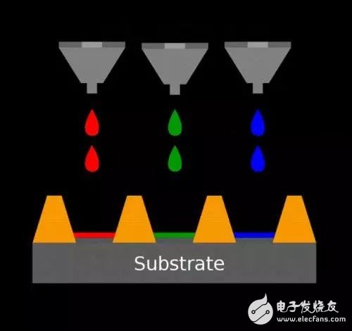
Graphical diagram of printed OLED implementation technology
According to industry sources, the biggest bottleneck in printed OLEDs is the differential control between each tiny printed dot (reducing the difference between pixels) and the development of devices for very small sub-pixel units (improving device accuracy). The former is a key bottleneck in the entire print display industry, while the latter is mainly a problem for small and medium size display products. In other words, for printing OLEDs, ink stability is not the ultimate big problem, equipment accuracy and stability is the real test. This problem must be solved in engineering only after the establishment of a demonstration production line.
Domestic Huaxing Optoelectronics, a number of printing and display backbone units in the United Nations, jointly established the country's first "printing display technology and material technology innovation alliance", set up a printing and flexible display public technology service platform, and with Guangdong Juhua Printing Display Technology Co., Ltd. as Platform operating entity.
Three implementations of OLED screen color
The above-mentioned high-end atmospheric grade "evaporation" method is mainly applied to a typical OLED screen of RGB three-color arrangement. Many of Samsung's OLED TV products are based on this method, and the effect is very good. The three primary colors are very pure, but the cost is very high. The technology used in this type of evaporation is called FMM, a fine metal mask, which is to cover the pixels and cover a mask during evaporation, so the alignment problem and the mask material itself become technical difficulties.
In fact, in order to control costs, humans have more than one kind of OLED TV. There is a type of blue light + color conversion layer: this scheme only needs to evaporate blue OLED components, and converts the light into RGB three colors through the conversion layer. The limitations of converter development have not been adopted on a large scale.
There is also a class of OLED TVs that are white light + three color filters, which are similar in principle to LCD liquid crystal panels, with white backlighting and color filters - this method is obviously much lower in cost, LG OLED TVs have been produced in this way. White OLEDs + color filters have also been considered as OLEDs to further realize low-cost solutions. Only with the addition of filters, the light color purity is more problematic, so the brightness, contrast, color, and energy-saving performance are theoretically inferior to RGB OLED.
AMOLED flat panel display development process and technical difficulties
The development of AMOLED technology mainly involves two aspects of TFT backplane and OLED device. In the choice of technical routes, there is currently no international unification, and a variety of technical solutions are under development.
The performance of the OLED, ie OLED, determines the color performance and power consumption of the AMOLED display. Therefore, the development of OLED device technology is of great significance to the improvement of product competitiveness. There are two key points in OLED device fabrication technology. One is to develop high mobility transmission materials and high efficiency, long life luminescent materials, and the other is to develop new device structures and improve device performance. Therefore, the development of new organic materials, the design of new device structures and the improvement of vacuum evaporation technology will be the focus of research.
At present, the channel layer semiconductor material in the TFT backplane mainly includes amorphous silicon (a-Si), microcrystalline silicon (μ-Si), low temperature polysilicon (LTPS), single crystal silicon, organic matter, and oxide. Since the OLED is a current-driven device, a stable current is required to control the luminescence characteristics. In order to achieve sufficient brightness, AMOLED requires a high mobility of the channel material of the TFT to provide a higher current density. Therefore, amorphous silicon TFTs currently commonly used in TFT-LCDs are difficult to meet due to low mobility. Claim. In addition, unlike the TFT-LCD, the AMOLED requires the TFT to be turned on for a long time, and the threshold voltage drift problem of the amorphous silicon TFT also makes it difficult to apply in the AMOLED. From the state of the art development, more promising is the oxide TFT and LTPS TFT technology, but there are many difficulties.
At present, the most mature TFT backplane technology used in AMOLED is low temperature polysilicon (LTPS) technology. In LTPS technology, the most important process difficulty is the preparation of polysilicon channel layer. In the process, a layer of amorphous silicon is first deposited on a glass substrate containing no alkali ions by means of PECVD, and then the amorphous silicon film is absorbed by laser or non-laser, and the atoms are rearranged to form a polysilicon structure. Reduce defects and get higher electron mobility.
For LTPS crystallization technology, laser crystallization technology, especially excimer laser annealing (ELA) technology, is now mature in small-size applications. The global production of AMOLED products has basically used ELA technology. The difficulty of ELA technology lies in the consistency problem of TFT. The difference in TFT characteristics between pixels leads to uneven illumination intensity of OLED, which leads to the inconsistency of panel yield. Therefore, the TFT consistency prepared by ELA technology has been the unit at home and abroad. The focus of research and development. In addition, ELA technology also has a large problem in mass production of large-sized substrates.
On the other hand, non-laser crystallization technology has great advantages in mass production of large-sized substrates and cost reduction, as well as in TFT uniformity. However, non-laser crystallization technology also has technical problems at this stage. Metal-induced crystallization (MIC) technology is difficult to solve defects and lifetime problems due to leakage current caused by metal contamination; solid phase crystallization (SPC) technology has a large comprehensive advantage in the preparation of large-size AMOLEDs. However, its carrier mobility is lower than that of laser crystallization technology, and it still needs further improvement in mass production technology.
AMOLED production process
The manufacturing process of LTPS-AMOLED includes many cutting-edge technologies in the display panel industry, which are mainly divided into three processes: the back plate segment, the front plate segment and the module segment. The back plate segment process forms a film of different materials of different patterns by film formation, exposure, etching to form an LTPS (low temperature polysilicon) driving circuit, which provides a lighting signal and a stable power input for the light emitting device. The technical difficulty lies in the micron-level process fineness and the extremely high uniformity requirement for electrical specifications.
The coating process is to use a coating device to physically or chemically deposit the desired material onto the glass substrate (2);
The exposure process is to adopt optical illumination to transfer the pattern on the photomask to the coated substrate (3, 4, 5) through the photoresist;
The etching process uses a chemical or physical method to etch away the film under the pattern that is not covered by the photoresist on the substrate, and finally washes off the photoresist on the cover film, leaving a film layer with the desired pattern (7, 8). ).
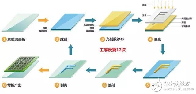
Drive backplane process flow chart
The front plate segment process evaporates the organic light-emitting material and the cathode material on the back plate through a high-precision metal mask (FMM), combines with the driving circuit to form a light-emitting device, and then encapsulates in an oxygen-free environment to protect the surface. . The alignment accuracy of the evaporation and the hermeticity of the package are the challenges of the front plate process.
High-precision metal mask (FMM): It is mainly made of materials with extremely low thermal deformation coefficient, which is the key to defining pixel precision. The finished FMM is accurately positioned on the metal frame by the netting machine and sent to the evaporation section (2);
The vapor deposition machine evaporates the organic material through the FMM onto the defined area of ​​the LTPS substrate under ultra-high vacuum (3);
After the evaporation is completed, the LTPS substrate is sent to the package section, and in a vacuum environment, it is bonded to the protective plate with a glass glue which is highly resistant to moisture. The choice of glass glue and its application in the manufacturing process will directly affect the life of OLED (5, 6).
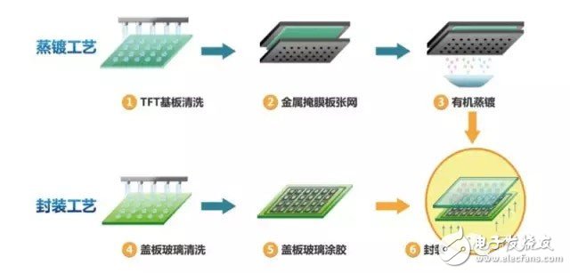
Organic coating section process flow chart
The module segment process cuts the packaged panel into the actual product size, and then performs various processes such as polarizer attachment, control circuit and chip bonding, and performs aging test and product packaging, and finally presents the product in the hands of the customer.
Cutting: the packaged AMOLED substrate is cut into a panel (1);
Panel test: perform panel lighting check (2);
Alignment: attach the AMOLED panel to the polarizing plate (3);
IC+FPC binding: link between driver IC and flexible printed circuit board (FPC) and AMOLED panel (4);
Attaching TP: AMOLED panel and strengthening the cover glass (cover Lens) containing bonded touch sensor (5);
Module test: aging test and lighting check of the module (6).
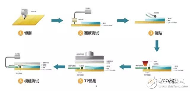
Module segment process flow chart
KNLN6-63 Residual Current Circuit Breaker With Over Load Protection
KNLN6-63 TWO FUNCTION : MCB AND RCCB FUNCTIONS
leakage breaker is suitable for the leakage protection of the line of AC 50/60Hz, rated voltage single phase 240V, rated current up to 63A. When there is human electricity shock or if the leakage current of the line exceeds the prescribed value, it will automatically cut off the power within 0.1s to protect human safety and prevent the accident due to the current leakage.
leakage breaker can protect against overload and short-circuit. It can be used to protect the line from being overloaded and short-circuited as wellas infrequent changeover of the line in normal situation. It complies with standard of IEC/EN61009-1 and GB16917.1.
KNLN6-63 Residual Current Circuit Breaker,Residual Current Circuit Breaker with Over Load Protection 1p,Residual Current Circuit Breaker with Over Load Protection 2p
Wenzhou Korlen Electric Appliances Co., Ltd. , https://www.korlenelectric.com