With the development of society, cars are more and more closely related to people's lives, and the DC voltage for automobiles is generally 12V, which cannot be used directly for portable electronic devices. For this reason, the development of vehicle power supply (that is, converting DC 12 V voltage into AC 220 V/50 Hz power supply) has attracted more and more attention.
This article refers to the address: http://
The traditional vehicle power supply generally adopts the scheme of processing the frequency transformer by the inverter, and has the defects of large volume and low efficiency. With the development of new power electronic devices and power electronics technology, the high frequency chain scheme is adopted to realize the inverter circuit without power frequency transformer, which can solve the problems of the traditional vehicle power supply and ensure the output voltage of the vehicle power supply is more stable. Smoother.
1 Car power circuit structure and function analysis
The vehicle power system is shown in Figure 1. The 12V DC voltage is subjected to high-frequency inverter and high-frequency rectification to obtain a satisfactory voltage: 350V DC voltage. The control signal of this part is generated by the TL494 chip.
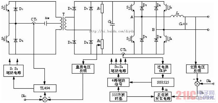
Figure 1 vehicle power system structure
After passing through the full-bridge DC/AC inverter circuit, a 220V/50Hz AC voltage output is obtained. In order to ensure the reliable operation of the system and prevent the main circuit from interfering with the control circuit, the main and control circuits are completely isolated, that is, the drive signals are isolated by optocouplers, the feedback signals are isolated by transformers, and the auxiliary power supplies are isolated by transformers.
For the entire system, whether the inverter circuit works properly determines whether the entire system can operate normally. Therefore, the focus of the design is on the control and detection of the inverter.
1.1 SG3525 block diagram and pin function
The system uses SG3525 to realize the output of SPWM control signal. The pin and internal block diagram of the chip are shown in Figure 2.

Figure 2 SG3525 pin and internal block diagram
The DC power supply Vs is divided into two paths after being connected from the pin 15, one is added to the NOR gate, and the other is sent to the input of the reference voltage regulator to generate a stable +5V reference voltage. +5V is then sent to other components of the internal (or external) circuit as a power supply.
The oscillator pin 5 must be connected to the external capacitor CT, and the pin 6 must be connected to the external resistor RT. The oscillator frequency f is determined by the external resistor RT and the capacitance CT, f=1.18/RTCT. The inverter bridge switching frequency is set to 10 kHz, taking CT=0.22 fog, RT=5k佟U竦 female î€ î€ hinge is sent to the flip-flop and two NOR gates in the form of clock pulses; the other way It is sent to the non-inverting input of the comparator in the form of a sawtooth wave, and the inverting input of the comparator is connected to the output of the error amplifier. The output of the error amplifier is compared with the sawtooth voltage in the comparator, and a square wave pulse that varies in width with the output voltage of the error amplifier is output, and the square wave pulse is sent to an input of the NOR gate. The other two inputs of the NOR gate are the flip-flop and the oscillator sawtooth. The two outputs of the flip-flop are complementary, alternately output high and low levels, and send PWM pulses to the bases of the transistors V1 and V2. The role of the sawtooth wave is to add dead time to ensure that V1 and V2 are not turned on at the same time. Finally, V1 and V2 respectively output PWM waves with phase differences of 180°.
1.2 SPWM modulation signal generation
To obtain the output of the sinusoidal voltage, the control signal of the inverter circuit is controlled by the SPWM mode to control the switching of the power tube, and the obtained pulse square wave output is filtered to obtain the sinusoidal output voltage. To achieve the output sinusoidal voltage through the SG3525, the SPWM modulation signal must be obtained first. To obtain the SPWM modulation signal, a sinusoidal wave with a magnitude of 1 to 3.5V and a sinusoidal variation must be added to the SG3525 pin 2 And compared with the sawtooth wave, a sinusoidal pulse width modulated wave can be obtained.
The block diagram of the control circuit that implements SPWM is shown in Figure 3(a). The waveform of each point of the actual circuit is shown in Figure 3(b).
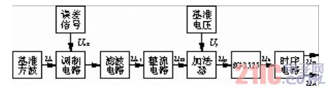
(a) SPWM control circuit block diagram
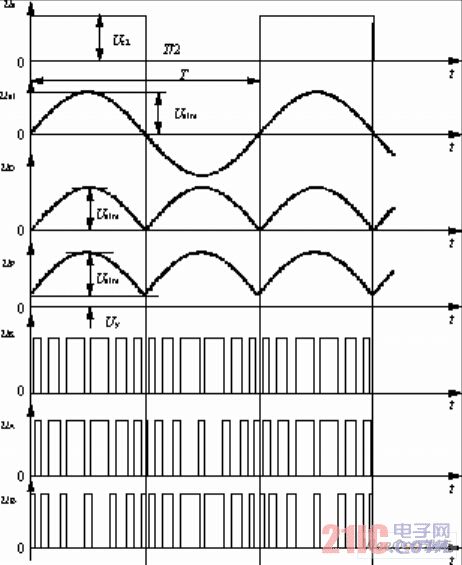
(b) Waveform of the main node of the SPWM circuit
Figure 3 control circuit block diagram and waveforms at each point
It can be seen from Fig. 3 that the square wave of the reference 50 Hz is generated by the 555 chip, and is used to control the error signal generated by comparing the effective value of the output voltage with the reference value, and convert it into a square wave of 50 Hz, and obtain sinusoidal control through low frequency filtering. signal. When the output voltage of the power supply changes, the amplitude of the sinusoidal signal is changed, so that the output pulse width of the SG3525 also changes accordingly, which constitutes a closed feedback loop, which can effectively stabilize the output waveform.
1.3 Overcurrent protection
Overcurrent protection uses a current transformer as a current sensing element, which has a fast enough response speed to turn it off during the overcurrent time allowed by the IGBT for protection.
As shown in Figure 1, the overcurrent protection signal is taken from CT2, divided and filtered, and applied to the non-inverting input of the voltage comparator, as shown in Figure 4. When the non-current detection signal of the non-inverting input is higher than the reference level of the inverting input, the comparator outputs a high level, which causes D2 to change from the original reverse bias state to the forward conduction, and raises the non-inverting terminal potential to high. The level makes the voltage comparator always output a high level. At the same time, the overcurrent signal is also sent to the foot 10 of the SG3525. When the pin 10 of the SG3525 is at a high level, the pulse width modulation pulse outputted on the leg 11 and the pin 14 immediately disappears to become zero.
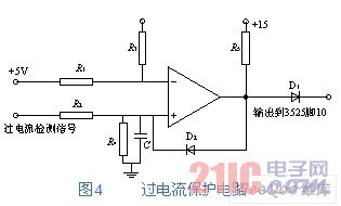
Figure 4 over current protection circuit
1.4 Drive circuit design
The design of the driving circuit should consider that the driving voltage can be quickly established when the power tube needs to be turned on, and the charge on the gate capacitance of the power tube can be quickly discharged when the power needs to be turned off, and the driving voltage is pulled down. . The specific drive circuit is shown in Figure 5.
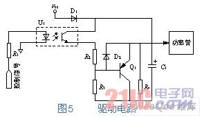
Figure 5 drive circuit
Its working principle is:
1) When the driving pulse current of the control circuit on the primary side of the optocoupler flows, the optocoupler is turned on, so that the base potential of Q1 rises rapidly, causing D2 to conduct, and the gate voltage of the power tube rises, so that the power tube is turned on;
2) When the driving pulse current of the optocoupler primary side without the control circuit flows, the optocoupler does not conduct, so that the base potential of Q1 is pulled low, and the voltage on the gate of the power tube is still high, so Q1 is turned on. The gate charge of the power tube is quickly discharged through Q1 and resistor R3, so that the power tube is quickly and reliably turned off.
Of course, the protection of the power tube is also important, so a buffer circuit is added between the source and the drain of the power tube to prevent the power tube from being damaged by excessive positive and negative voltages.
2 Experimental results
According to the above analysis, the experimental prototype was tested. The rated output power was 500W, the filter parameters were L=3mH, C=2.2 fog. When the prototype was running with load, the output voltage waveform was measured as shown in Fig. 6.

Figure 6 inverter output waveform
3 Conclusion
The output voltage waveform of the prototype is of good quality, the output voltage is stable, and the amplitude is basically not affected by the load change, and the effect is good. Experiments show that the system proposed in this paper is feasible.
Welding diodes are available for medium frequency (over 2KHz) and high frequency (over 10khz) applications.They have very low on - state voltage and thermal resistance. Welding diodes are designed for medium and high frequency welding equipment and optimized for high current rectifiers. The on-state voltage is very low and the output current is high.
Welding Diode,Disc Welding Diode,3000 Amp Welding Diode,High Current Rectifier Welding Diode
YANGZHOU POSITIONING TECH CO., LTD. , http://www.yzpst.com