As an important circuit unit in analog systems and mixed-signal systems, op amps are widely used in various circuits such as digital-to-analog and analog-to-digital converters, active filters, waveform generators, and video amplifiers. With the development of each generation of CMOS technology, the continuous reduction of the supply voltage and transistor channel length has repeatedly raised complex issues for the design of operational amplifiers. In an A/D converter, an op amp is the most critical component. For example, non-ideal characteristics of op amps such as finite gain, bandwidth, and finite slew rate can cause incomplete charge transfer in the integrator, causing nonlinearity in the A/D converter. Compared to single-ended output op amps, fully differential op amps provide greater output voltage swing and are less susceptible to common mode noise, higher linearity, reduced even harmonic interference, and bias circuitry. Simple and other advantages.
In this paper, from the analysis and optimization of the parameters of the operational amplifier, a high-performance CMOS fully differential operational amplifier is designed. The main performance requirements are as follows: open loop gain greater than 70dB, unity gain bandwidth greater than 80 MHz, conversion rate greater than 160 V /μs.
2 High Gain CMOS Fully Differential Operational Amplifier Design 2.1 Structure Selection and AnalysisCommon fully differential operational amplifiers are available in a sleeve cascode, a folded cascode, and a two-stage op amp. In the two-stage op amp structure, the secondary pole frequency is determined by the load capacitance CL, which limits the speed, the bandwidth is small, and the power consumption is large, and the power supply rejection ratio and the common mode rejection ratio are also poor. The output voltage swing of a folded cascode op amp is larger than that of a telescopic structure, but this is at the expense of greater power consumption and noise, lower voltage gain, and pole frequency [ 2]. Sleeve cascode is one of the lowest power consumption of various op amp structures, and its gain is also high, which can be compared with ordinary two-stage op amps. From the application of this design, it was decided to design a fully differential operational amplifier using a sleeve cascode structure.
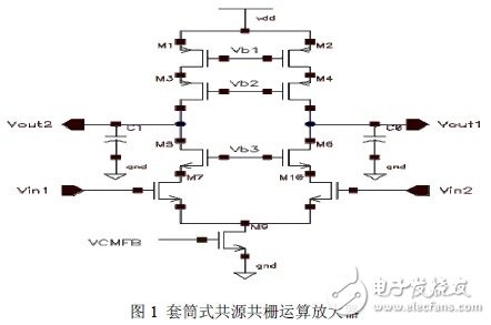
2.2 Sleeve cascode operational amplifier The main structure of the sleeve type cascode operational amplifier used is shown in Figure 1. Among them, M1, M2, M3 and M4 form an active load, which has a large resistance value and can improve the gain of the operational amplifier. M7 and M8 are NMOS differential input pairs that are used to convert the input voltage into current; M7, M8 and M5, M6 together form a differential cascode structure. M9 is used to generate tail current to suppress the effect of changes in the input common-mode level on the operation and output levels of M7 and M8. Vb1, Vb2, and Vb3 are three bias voltages, and VCMFB is the control voltage generated by the common mode feedback circuit.
A common-mode feedback circuit (CMFB) is typically required in fully differential op amps to bring the controlled common-mode output voltage close to a certain value (usually about half the supply voltage) [4]. CMFB is divided into continuous time and switched capacitor. Since the op amp designed in this paper is used in the fully differential switched capacitor circuit, and the continuous time CMFB has the disadvantages of limiting the amplitude of the differential mode output signal, increasing the differential mode load and increasing the static power consumption [5-6], the switched capacitor CMFB is used. The actual structure is shown in Figure 2.
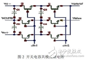
In Figure 2, C1=C2, C3=C4, clk1 and clk2 are two-phase non-overlapping clock signals, Vo- and Vo+ are connected to the op amp output voltage, VCMFB is the regulated voltage generated by the CMFB, and Vcmref represents the desired output common mode. The voltage, Vbias, is the current source gate bias when the op amp's output common-mode voltage is exactly equal to the desired value. When clk2 is high, C3 and C4 are precharged to Vcmref-Vbias. When clk1 is high, C1 and C3 are connected in parallel, C2 and C4 are connected in parallel, the charge stored on C3 and C4 will be transferred, and finally a DC compensation voltage is generated between C1 and C2, superimposed on the output common mode of the op amp. On the voltage, to ensure that the op amp's actual output common-mode voltage remains near the expected value.
3 circuit parameter analysis In the circuit shown in Figure 1, since the two branches are symmetrical, when the differential mode AC signal is input, the drain potential of M9 is kept constant, so the drain of M9 can be considered to be AC ​​grounded, thereby obtaining the single of Figure 1. The AC signal equivalent circuit is shown in Figure 3.
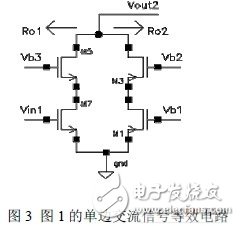
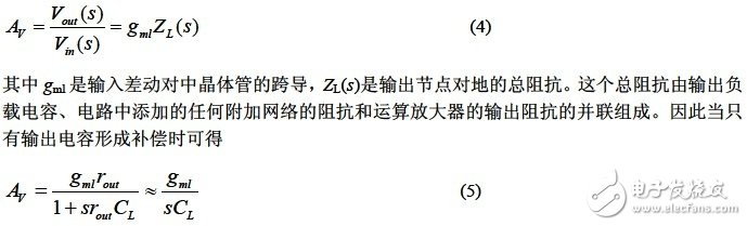
As shown in Figure 3, the unilateral gain is equal to the transconductance of the input tube multiplied by the output resistance. The output resistance is equal to the parallel connection of the two cascode output resistors seen from the output node, so there is
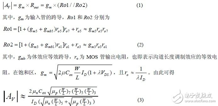
The above equation points out the contribution of a particular transistor to the DC gain of the circuit, and is therefore the overall guiding basis for transistor parameter adjustment. In addition, as can be seen from Figure 1, M5, M6, M7 and M8 are in the signal path, so to ensure that the capacitance value is the smallest, so in the process of changing the parameters to increase the DC gain, try to keep the minimum size unchanged. Make an overall change in the aspect ratio. The PMOS transistors M1, M2, M3, and M4 have much less influence on the signal, and increasing their size can very effectively change the DC gain.
3.2 unity gain bandwidthThe small signal transfer function of the telescopic cascode op amp can be written as
It can be seen from equations (3) and (10) that increasing the W/L of the input differential tube and reducing the load capacitance are effective methods for increasing the unity gain bandwidth.
3.3 Conversion rate and settling timeWhen the op amp is rated for load and the input step is large, the slope of the linear portion of the rising (or falling) portion of the output voltage is called the slew rate, also called the slew rate. Figure 1 shows the slew rate SR=ID9/CL of the op amps Vout1-Vout2. In this design, the load capacitance CL is 2.6 pF and the slew rate is required to be greater than 160 V/μs, so the ID9 is at least 0.42 mA.
Settling time refers to the time required for the output voltage to flow from the step signal input to the error tolerance of the output voltage to the stable value when the operational amplifier forms a closed-loop negative feedback under the condition of limiting the output load and inputting the step signal. . It is divided into two different stages: linear establishment and nonlinear establishment. The linear setup phase refers to the phase in which the output of the op amp is controlled by the closed loop when the differential small signal is input. The larger the unity gain bandwidth, the shorter the linear settling time. The nonlinear setup phase refers to the phase in which the output waveform of the operational amplifier is determined by the slew rate when the differential large signal is input, so this time can be shortened by appropriately increasing the tail current.
3.4 Common mode input range The input common-mode voltage range is defined as the range of common-mode levels that maintain the circuit operating in the saturation region when the differential signal is zero. For an ideal differential op amp, the output should be zero when the common-mode voltage is input. With an actual differential op amp, the circuit is not completely symmetrical, and the output impedance of the tail current source is not likely to be infinite. Therefore, the output is not zero when the common mode voltage is input; even when the input common mode voltage exceeds a certain range, the op amp can no longer normally amplify the differential mode signal. As can be seen from Figure 1, the input common mode voltage VIC has:
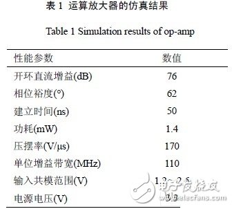
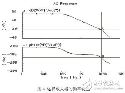
The CMOS operational amplifier was simulated on a Cadence Spectre simulator based on a SMIC 0.35 μm CMOS process. The results are shown in Table 1. Figure 4 shows the frequency response characteristics of the op amp.
A simple-sleeve cascode structure is used to analyze a variety of factors that determine the main performance parameters such as open-loop DC gain, unity gain bandwidth, slew rate, and settling time. A fully-performing differential amplifier with excellent performance is realized. Spectre simulations show that the performance specifications of the op amp meet the design requirements and can be applied to high-precision audio Σ-Δ A/D converters.
Solar Panel Controller Mppt,Mppt Solar Charge Controller 80A 48V,Controlador De Carga Solar Mppt,Solar Charge Controller 80A
GuangZhou HanFong New Energy Technology Co. , Ltd. , https://www.gzinverter.com