1 Introduction
Programmable logic devices (PLDs) are the next generation of digital system logic devices popular in the world. It is mainly a "and-or" two-stage structure device. In addition to its high speed and high integration performance, its biggest feature is that users can define its logic functions. Therefore, PLD can adapt to various needs, greatly simplify system design, reduce system scale, improve system reliability, and is favored by engineers and technicians.
There are many different types of programmable logic devices, and there are several basic types: Programmable Read Only Memory (PROM), Field Programmable Logic Array (FPGA), Program Array Logic (PAL), General Array Logic (GAL). . Generic ArrayLogic (GAL) is a new generation of programmable logic devices. It is a large-scale integrated circuit fabricated by advanced E2CMOS technology and is an ideal device for new product design. The user can program the logic circuit through the IBM-PC machine to program the GAL chip. The programming process can be divided into three steps: (1) writing Boolean equations with or logical expressions according to design requirements; (2) using a compiler, computer-aided programming, obtaining the fuse map of the array, and verifying its correctness; (3) The output of the compiler is sent to the programmer due to the immediate electrical erasability of the GAL. The programmer stores the new internal structure information in accordance with the determined fuse map. This programming method is simple and easy.
2 system composition and system design
2.1 System composition
The system we introduced is a high-accuracy A/D converter based on two samples. It has a counting capacity of up to two million yards, which is equivalent to a six-and-a-half-digit A/D converter. It is a high-accuracy A/D converter that can be done in China at present. Its working principle is to sample the signal under test twice: the first sampling is converted into the corresponding digital quantity N2h by the double integral type A/D converter. The timing integration time of the second sampling is extended by m times than the timing integration time of the first sampling, and the corresponding reference voltage is periodically turned on to the summing integrator by N2h. When the integral is integrated, the small reference voltage Es/n is used for discharging, so that the reading N2l corresponding to the low position of the measured signal is obtained. Combining the two sampling results, the total value of the A/D converter is: mnN2h+N2l. Its overall block diagram is shown in Figure 1.
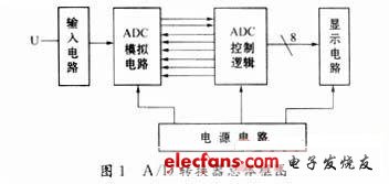
Since the system needs a large logic control circuit to complete the two sampling process, we use PLD to implement the hardware control logic.
2.2 System design
Among all PLDs, GAL devices are selected for high accuracy because of their low power consumption, high speed, reprogrammable and output reconfigurable features, and their cost performance is significantly better than SSI/MSI devices. The hardware logic control circuit of the /D converter.
2.2.1 Hardware logic control circuit
The GAL16V8 chip has five main output configuration functions. The combined output structure and register output structure in its register type device are used in the design. The GAL16V8 chip we use is shown in Figure 2.
Its various pins are defined as follows:
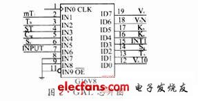
mT1: Timing time signal for timing integration (active low), Th: feedback timing signal (active low), ST: ADC conversion enable signal (active edge is active), Sc: secondary sampling signal (high level) Valid), INPUT: Zero detection signal input (0 when Ux>0, 1 when Ux<0), Tx: Result count output (active high), Sg: Polar output (0 when Ux>0, Ux<0 is 1), INT1: Interrupt signal (active edge is valid), Kc: Discharge loop control (active high), Kx: measured access control (active high), VrN: negative reference In control (active high), Vr: positive reference access control (active high), Vr-10: one tenth positive reference (active high), Csg: release polarity output register (high power) Flat valid), CLK: clock input.
2.2.2 Hardware logic control circuit working process
When the hardware logic circuit is working, the A/D conversion enable signal ST changes from "0" to "1", indicating that the first sampling is officially started. At the same time, Kx goes high, indicating that the access is measured Ux; mT1 goes low, and the system enters the timing integration time of the first sampling. Assuming Ux>0, the zero detection signal INPUT is "0". When mT1 goes high, the timing integration time of the first sampling ends. Access VrN and enter the quantitative integration phase of the first sampling. When the zero detection signal changes, it indicates that the quantitative integration is over. In the process of quantitative integration, Tx has a count result output, which is the high value of the signal under test. The interrupt signal INT1 changes from "1" to "0", indicating that the first sampling ends and the system enters the rest phase. When the ST and the subsampled signal Sc simultaneously generate a positive edge, the system enters the second sampling phase. During the second sampling process, the logic control process is approximately the same as the first sampling, except that the timing integration time becomes m times the first sampling timing integration time, ie mT1, and is turned on during each T1 time. Feedback timing signal Th. In the fixed value integration phase, the small reference voltage Vr-10 is used instead for discharging. Thus Tx has a count result output, which is the low value of the signal under test. At this point, the two-sample A/D conversion ends.
2.2.3 Hardware logic control circuit timing diagram
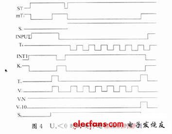
The key to designing a control circuit using a programmable logic device is to correctly plot the timing diagram of the logic circuit. Draw the timing diagram of the A/D converter by accurately analyzing the logic of the two-sampling A/D converter.
(1) When the measured voltage is positive, the timing chart of each GAL pin is shown in Figure 3.

(2) When the measured voltage is negative, the timing chart of each GAL pin is shown in Figure 4.
3 GAL Programmable Device Program
According to the hardware logic circuit timing diagram, the GAL16V8 chip is now programmed to complete the above logic functions.
4 Conclusion
The waveform output from each pin of the GAL16V8 chip is observed by an oscilloscope to obtain a correct waveform output. Comparing the data measured after using GAL with the data measured by the original logic circuit, it is proved that the data obtained by using GAL is completely correct. Therefore, it is feasible to design a hardware logic control circuit of a high-accuracy A/D converter by GAL. In addition, since the GAL has only one clock control terminal, in order to reduce the error caused by the clock when the signal is operating, the clock frequency used is higher than twice the counter clock frequency. The higher the clock frequency, the smaller the error.
Compared with general logic circuits, GAL not only ensures the correctness of the system, but also improves the confidentiality and reliability of the system.
At Christmas it is nice, in addition to the tree decorated with
large and colorful Christmas balls, to surround yourself with
decorations with Christmas motifs to be distributed around the house.
Create the right atmosphere with this led light garland.
Portable & Versatile
1.The item have a base and could stand on anywhere.
2.Integrated hanging hook holes for ease of display on wall or just rest on mantle, self, table or dresser.
3.Can be displayed standalone or combined with other pieces to create an eclectic lighting installation.
3.Create a whimsy showpiece on the cake or candy table during the Wedding.
Christmas Motif Lights,Led Motif Light,Christmas Motif Led Rope Light,Christmas Motif Light Decoration
XINGYONG XMAS OPTICAL (DONGGUAN ) CO., LTD , https://www.xingyongled.com